-
In recent years, flash-based SSDs have grown enormously both in capacity and popularity. In highperformance enterprise storage applications, accelerating adoption of SSDs is predicated on the ability of manufacturers to deliver performance that far exceeds disks while closing the gap in cost per gigabyte. However, while flash density continues to improve, other metrics such as a reliability, endurance, and performance are all declining. As a result, building larger-capacity flashbased SSDs that are reliable enough to be useful in enterprise settings and high-performance enough to justify their cost will become challenging. In this work, we present our empirical data collected from 45 flash chips from 6 manufacturers and examine the performance trends for these raw flash devices as flash scales down in feature size. We use this analysis to predict the performance and cost characteristics of future SSDs. We show that future gains in density will come at significant drops in performance and reliability. As a result, SSD manufacturers and users will face a tough choice in trading off between cost, performance, capacity and reliability.
The technology trends we have described put SSDs in an unusual position for a cutting-edge technology: SSDs will continue to improve by some metrics (notably density and cost per bit), but everything else about them is poised to get worse. This makes the future of SSDs cloudy: While the growing capacity of SSDs and high IOP rates will make them attractive in many applications, the reduction in performance that is necessary to increase capacity while keeping costs in check may make it difficult for SSDs to scale as a viable technology for some applications.
Via: http://cseweb.ucsd.edu/users/swanson/papers/FAST2012BleakFlash.pdf
-
There is already a succesor for the SSD:
CAM to be the next big thing after SSD?
We just started to see the power of the SSD, and they already started working on a new medium that will be a thousand times as quick, more responsive and will consume less power than the current SSD. It is likely that it will take some time before this new medium will become mainstream, but that it will be coming sooner or later is a fact. This is if the news that is released about these so-called CAM chips is based on the truth. The chips are considered to be the next big thing after SSD.
CAM stands for Content Addressable Memory and has a read speed that is comparable to today’s internal memory chips eg DDR memory. There is also one big advantage in comparison with standard RAM memory, the chips no longer need power running through the memory to save the data. This technique makes it possible to use them as a fast storage medium. The CAM system only needs to be powered when you want to change file system, reading data doesn’t require any energy of the chip making it ideal for use in laptops like the MacBook Air.
NEC and Japan’s Tohoku University develop the CAM system. Later this week they will be showing their latest results in a presentation.
via http://www.yourdailymac.net/2011/06/cam-to-be-the-next-big-thing-after-ssd/
I read CAM memory will be cheaper than SSD on the German CHIP newspaper. they presented it a year ago, will see when comes to the market..
-
If you ask me. I think all approach to non-volatile memory is fucked up.
All I really need is non-erasable non-destructable high density stuff. Minimum 500 thousands years guaranteed.
-
Unfortunately I have not technically very thorough knowledge on the subject, I have to believe what the newspapers write. They make for every smallness the new imminent big thing.
-
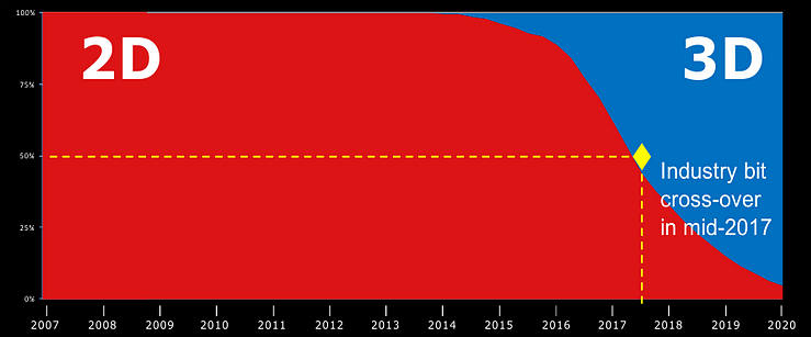
Non-volatile memory storage systems have short market life times. If we go back to 8" floppies, 5 1/4" floppies, 3 1/2" floppies, CD, DVD, BluRay and what ever comes next - each generation lasted a relatively short period of time. While we still have CD/DVD/BluRay, those are already fading due to use of hard drives (or Flash or SSD) and broadband networks for content delivery.
As the paper authors suggest, perhaps SSDs are approaching their peak success and we will all move on to the next technology, which could be CAM.
-
Find a way to store in deinococcus radiodurans matrix... 500 million years!
-
Jeff Bezos' 10,000-year clock:
http://www.wired.com/gadgetlab/2011/06/10000-year-clock/all/1
-
Interesting SSD endurance test
We started with six SSDs: the Corsair Neutron GTX 240GB, Intel 335 Series 240GB, Samsung 840 Series 250GB, Samsung 840 Pro 256GB, and two Kingston HyperX 3K 240GB. They all exceeded their endurance specifications early on, successfully writing hundreds of terabytes without issue. That's a heck of a lot of data, and certainly more than most folks will write in the lifetimes of their drives.
The casualties didn't die in vain. They showed little performance slowdown toward the ends of their lives, suggesting SSDs can keep up the pace until the very end. And they showed us that drives can expire in different ways. The Intel 335 Series checked out voluntarily, at a predetermined cycle limit, while the Kingston HyperX 3K tried to squeeze every last drop out of the flash. Both provided ample warning of their demise and enough headroom for users to back up their data.
The Samsung 840 Series died suddenly, but the writing had been on the wall for a while in the form of mounting block failures. Some of those failures may have been responsible for the uncorrectable errors that struck during the drive's life. The 840 Series' error correction apparently wasn't strong enough to overcome a few hurdles, albeit ones that didn't arise until after hundreds of terabytes of writes.
Given our limited sample size, I wouldn't read too much into exactly how many writes each drive handled. The more important takeaway is that all of the SSDs, including the 840 Series, performed flawlessly through hundreds of terabytes. A typical consumer won't write anything close to that much data over the useful life of a drive.
http://techreport.com/review/26523/the-ssd-endurance-experiment-casualties-on-the-way-to-a-petabyte
-
Next part of endurance test
Our experiment began with the Corsair Neutron GTX 240GB, Intel 335 Series 240GB, Samsung 840 Series 250GB, and Samsung 840 Pro 256GB, plus two Kingston HyperX 3K 240GB drives. They all surpassed their endurance specifications, but the 335 Series, 840 Series, and one of the HyperX drives failed to reach the petabyte mark. The remainder pressed on toward 1.5PB, and two of them made it relatively unscathed.
Modern SSDs appear to have more than enough endurance for typical client workloads. All six of our subjects wrote hundreds of terabytes without issue, which is far more data than even most power users will need to write during the useful lives of their drives.
The 840 Pro and remaining HyperX are already on their way to 1.6PB.
http://techreport.com/review/27062/the-ssd-endurance-experiment-only-two-remain-after-1-5pb
-
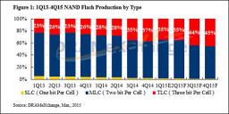
News are not very good

TLC memory with tiny amount of writing cycles and overall resource is winning.
 sales129.jpg523 x 262 - 36K
 -
I have a samsung 840 evo, which is TLC. If you are not aware already, there is some kind of issue where the drive read speeds slow down after 1-3 months time. Samsung already tried to fix it, but only improved the read speeds to last for 3 months before speeds begin to drop again. You can see 60% or greater drop in read speeds. Expect to see this issue back in the news when samsung releases a second firmware/software "fix" and it does not improve the issue. There will be large public outcry.
-
You can see 60% or greater drop in read speeds. Expect to see this issue back in the news when samsung releases a second firmware/software "fix" and it does not improve the issue. There will be large public outcry.
Well, it is first bird. I think it is EVO as Samsung use defective chips (with mapped out bad parts) for it to keep margins good.
-
Things are not so good, if you store SSD, or keep it without power.
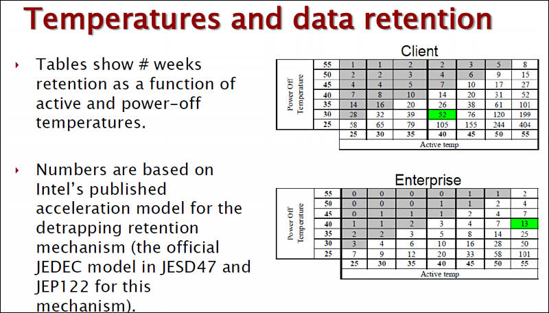
http://www.jedec.org/sites/default/files/Alvin_Cox%20%5BCompatibility%20Mode%5D_0.pdf
 dog_40.jpg800 x 437 - 53K
 dog_41.jpg800 x 456 - 86K
 -
If you’re in a panic because the Internet told you that your shiny new SSD may lose data in “just a few days” when stored in a hot room, take a chill pill—it’s apparently all a huge misunderstanding, according to the man who wrote the original presentation all the fear is based on.
In a conversation with Kent Smith of Seagate and Alvin Cox, the Seagate engineer who wrote the presentation that set the Internet abuzz, PCWorld was told we’re all just reading it wrong.
“People have misunderstood the data that they’re looking at,” Smith said.
Cox agreed saying there’s no reason to fret.
“I wouldn’t worry about (losing data),” Cox told PCWorld. “This all pertains to end of life. As a consumer, an SSD product or even a flash product is never going to get to the point where it’s temperature-dependent on retaining the data.”
For the rest of the artice, go to: http://www.pcworld.com/article/2925173/debunked-your-ssd-wont-lose-data-if-left-unplugged-after-all.html
-
“I wouldn’t worry about (losing data),” Cox told PCWorld. “This all pertains to end of life. As a consumer, an SSD product or even a flash product is never going to get to the point where it’s temperature-dependent on retaining the data.”
Well it is bullshit.
Actually most of PCWorld article is bullshit.
One thing that any SSD manufacturer do not want to tell you is that all recent price progress is accompanied with move to TLC chips in many drives and simple fact that big sizes, improved error correction and reserves do not show you fast degradation.
Take Samsung 840 evo (posts above), actual research showed that Samsung actually lied about it being firmware issue. With their fixes being mostly rewrites of big chunks of old data (see, matches with report) due to degradation. Also tests made by users showed that performance is temperature dependent.
-
Btw state of flash memory actually improved, as 3D TLC cells are significantly larger compared to planar TLC.
But QLC follows soon
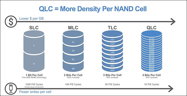
Toshiba announced the world’s first QLC — quadruple-level cell — 4-bit flash memory in a 3D flash device.
QLC allows even greater storage capacity by dividing each cell into 16 charge levels for four bits of data in each cell. For a while, it looked like reaching that level from TLC would be difficult; the level of precision in manufacturing needed to be able to accurately differentiate between charge levels increases exponentially. But Toshiba has pulled it off for its latest 3D NAND memory, which features 64-layer stacked QLC cells.
The QLC method allowed to reach 768 gigabit die capacity, a dramatic improvement over the earlier 512 gigabit TLC dies. New QLC dies can be stacked in a 16-die package to create a single chip device with 1.5TB of storage.
-
Interesting things:
First is electrons per one level difference (SLC has two levels, MLC - 4, etc)
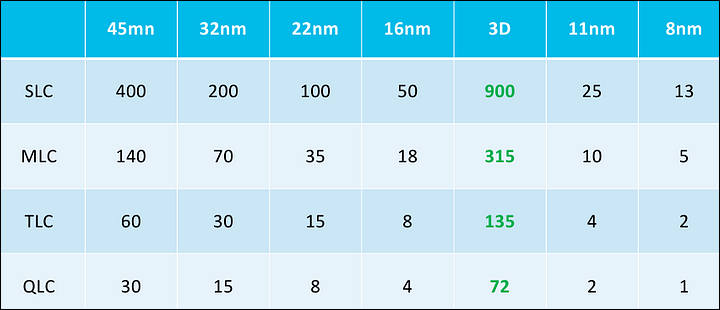
As you can see in 8nm and QLC memory it becomes one electron :-)
So, industry actually required 3D
 s1070.jpg720 x 310 - 31K
 s1071.jpg739 x 307 - 29K
 -
3D NAND issue
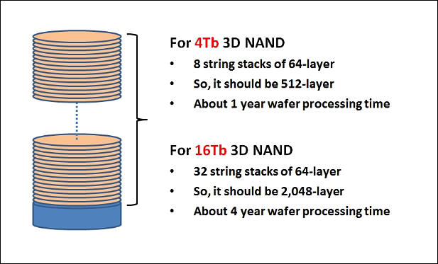
In order to implement the 4Tb NAND chip you need
- Eight string stacks of 64-layer are needed. Which will make (512Gb x 8) = 4Gb
- The total layer then becomes 512-layer on 130mm2 die size
- It will take about a year to process a wafer, 5 weeks for memory logic plus 8 times (i.e. 8 string stack of 64-layer) 5 to 6 weeks for a 64-layer cell layer implementation. Therefore, the wafer processing time for a 512-layer will be about 45 to 53 weeks.
It is practically impossible to implement the 4Tb NAND chip. If QLC is considered instead of TLC, there will be an improvement of 25 percent at best. So, a 410-layer will be needed for QLC 4Tb 3D NAND and about nine months of wafer processing time.
How about 16Tb 3D NAND? It needs 2,048-layers with four years of wafer processing time.
 s1367.jpg617 x 373 - 39K
 -
QLC 3D NAND coming
Micron Technology and Intel announced joint production and shipments of industry's first 4bits/cell 3D NAND technology. Leveraging a proven 64-layer structure, the new 4bits/cell NAND technology achieves one terabit (Tb) density per die.
"With introduction of 64-layer 4bits/cell NAND technology, we are achieving 33% higher array density compared to TLC, which enables us to produce the first commercially available 1 terabit die in the history of semiconductors".
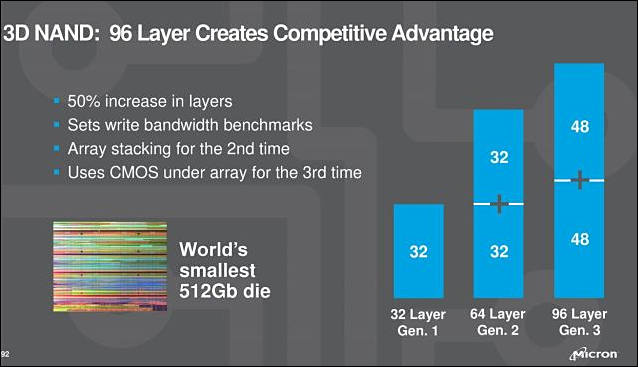
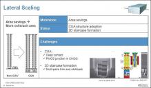
Theyannounced development progress on the third-generation 96-tier 3D NAND structure, providing a 50% increase in layers. Both NAND technology advancements - the 64-layer QLC and 96-layer TLC technologies - utilize CMOS under the array (CuA) technology to reduce die sizes and deliver improved performance when compared to competitive approaches.
-
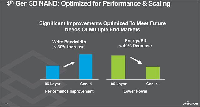
Micron slides about 96 layer memory and their 4th gen chips
 sa3371.jpg638 x 367 - 36K
 sa3372.jpg640 x 342 - 27K
 -
First SSDs that use 3D QLC spotted at Computex
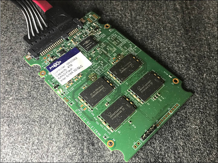
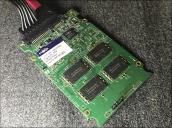 sa3568.jpg721 x 538 - 130K
 -
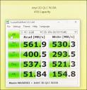
Speed is not so bad
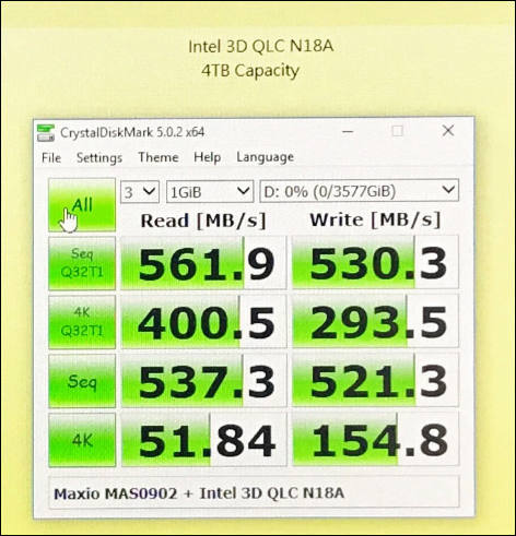
Check more - https://www.anandtech.com/show/12944/next-gen-storage-we-found-a-prototype-4-tb-intel-qlc-ssd-500-cycles
 sa3578.jpg472 x 491 - 49K
 -
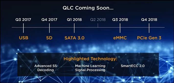
QLC push begins
The observers identified 2018 as the year when the industry is ready for volume production of QLC SSDs.
Samsung Electronics introduced recently the availability of consumer SSDs utilizing QLC 3D NAND technology. In mid-2018, Micron Technology and Intel announced jointly their QLC 3D NAND technology for mainly datacenter and other enterprise applications.
-
Chipmakers are encountering low manufacturing yield rates of 3D 4bits/cell (QLC) NAND chips, and substandard chips due to the poor QLC NAND yields may cause disruption to the market and further confusion in the memory pricing during the first half of 2019, according to industry sources
At least some delay.


Howdy, Stranger!
It looks like you're new here. If you want to get involved, click one of these buttons!
Categories
- Topics List23,992
- Blog5,725
- General and News1,354
- Hacks and Patches1,153
- ↳ Top Settings33
- ↳ Beginners256
- ↳ Archives402
- ↳ Hacks News and Development56
- Cameras2,367
- ↳ Panasonic995
- ↳ Canon118
- ↳ Sony156
- ↳ Nikon96
- ↳ Pentax and Samsung70
- ↳ Olympus and Fujifilm101
- ↳ Compacts and Camcorders300
- ↳ Smartphones for video97
- ↳ Pro Video Cameras191
- ↳ BlackMagic and other raw cameras116
- Skill1,960
- ↳ Business and distribution66
- ↳ Preparation, scripts and legal38
- ↳ Art149
- ↳ Import, Convert, Exporting291
- ↳ Editors191
- ↳ Effects and stunts115
- ↳ Color grading197
- ↳ Sound and Music280
- ↳ Lighting96
- ↳ Software and storage tips266
- Gear5,420
- ↳ Filters, Adapters, Matte boxes344
- ↳ Lenses1,582
- ↳ Follow focus and gears93
- ↳ Sound499
- ↳ Lighting gear314
- ↳ Camera movement230
- ↳ Gimbals and copters302
- ↳ Rigs and related stuff273
- ↳ Power solutions83
- ↳ Monitors and viewfinders340
- ↳ Tripods and fluid heads139
- ↳ Storage286
- ↳ Computers and studio gear560
- ↳ VR and 3D248
- Showcase1,859
- Marketplace2,834
- Offtopic1,320
Tags in Topic
- ssd 15


