It allows to keep PV going, with more focus towards AI, but keeping be one of the few truly independent places.
-
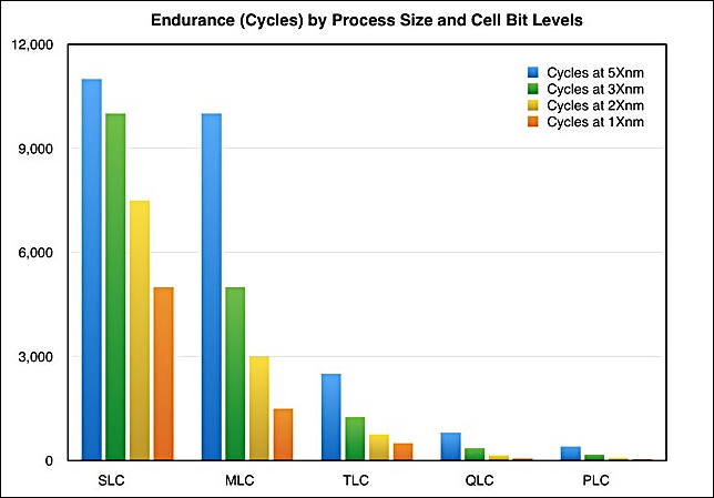
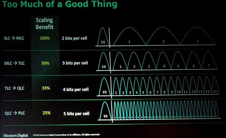
QLC comes finally
-
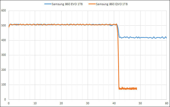
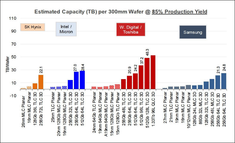
Tragedy of Samsung
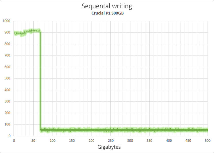
Writing large stuff
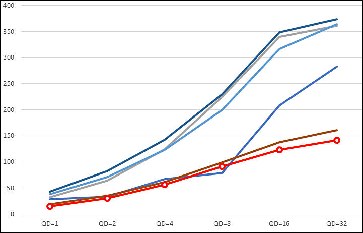
Random read (worst lines)
 sa5838.jpg669 x 422 - 37K
 sa5839.jpg721 x 462 - 43K
 -
Intel 660p. Horrible shit with writing speed.
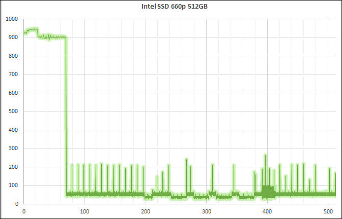
 sa6635.jpg672 x 432 - 42K
 -
WARNING! MICRON Plans To Introduce Octa-Level (OLC) NAND
Octa-Level Cell (OLC) NAND tech from Micron will feature 8 bits per cell for a 100% increase over QLC (per cell) and will be the first tech to essentially feature 1 byte per cell. This jump in density is something that will well exceed Moore’s Law (assuming the cell size does not increase too dramatically) and be a push for the industry and force the competition to play catch-up as well. SSD pricing for consumers will also almost certainly improve over the long term.
https://wccftech.com/exclusive-micron-octa-level-cell-tech-olc-nand-memory/
-
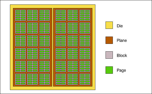
Toshiba on QLC memory and 128 layer TLC NAND
QLC cheap NAND memory will be 96 layer one.
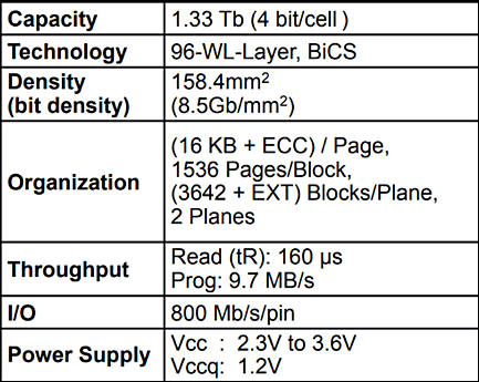
And TLC will move to 128 layer (now it is 64 layer!) organization with 4 planes:
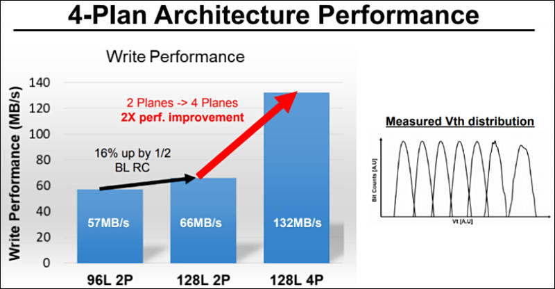
Sample of NAND organization (with 2 planes):
-
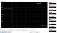
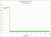
Situation on small disks - how about 14Mb/sec write speeds?
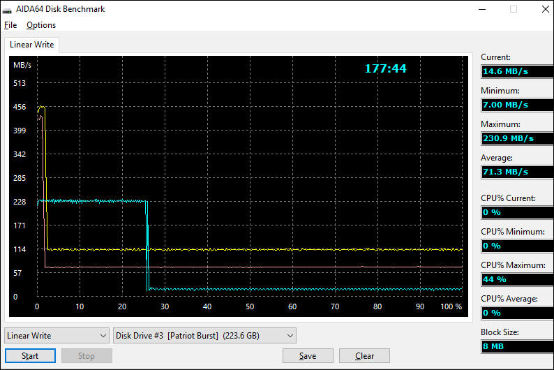
Cyan here is QLC drive write speed (first fast part is SLC caching) :-)
 sa7750.jpg794 x 530 - 89K
 -
SK Hynix applies its own QLC technology to 96-layer charge-trap-flash-based 4D NAND flash, said the company, adding that its 96-layer-based 1Tb QLC products will be "in time for the QLC market opening.
According to IDC, the proportion of QLC in the NAND Flash market is expected to increase from 3% in 2019 to 22% in 2023, while the eSSD market will grow at a CAGR of 47.9% to rapidly replace HDD during the five-year period.
-
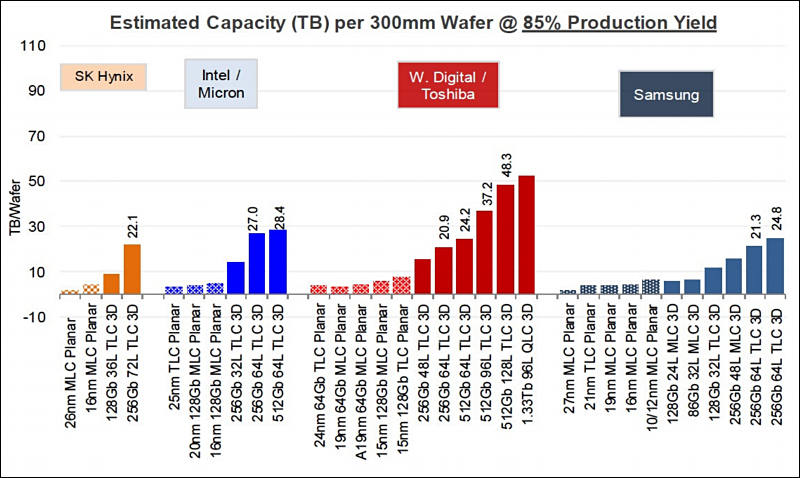
More QLC memory and 128 layer 3D TLC are being made
 sa8672.jpg800 x 478 - 77K
 -
SK Hynix indicated its 128-layer 1Tb NAND chip offers the industry's highest vertical stacking with more than 360 billion NAND cells, each of which stores three bits, per chip.
Hynix will start shipping 128-layer 4D NAND flash in the second half of 2019, according to the company.
SK Hynix intends to enter mass production of 2TB client SSDs with in-house developed controller and software in the first half of 2020, the company said. It added 16TB and 32TB NVMe SSDs for cloud data centers will also be released next year.
-
PLC coming
Fear and trembling (c)
Common 512Gb QLC SSD already has 30-50Mb/sec sustained write speed.
New ones can have 5-15Mb/sec sustained write speed, in the ballpark on late 198x HDDs.
 sa9529.jpg644 x 449 - 37K
 sa9530.jpg741 x 453 - 58K
 -
Toshiba proposal to double density by splitting each cell.
Write endurance can drop around 3-5x, but no one cares.
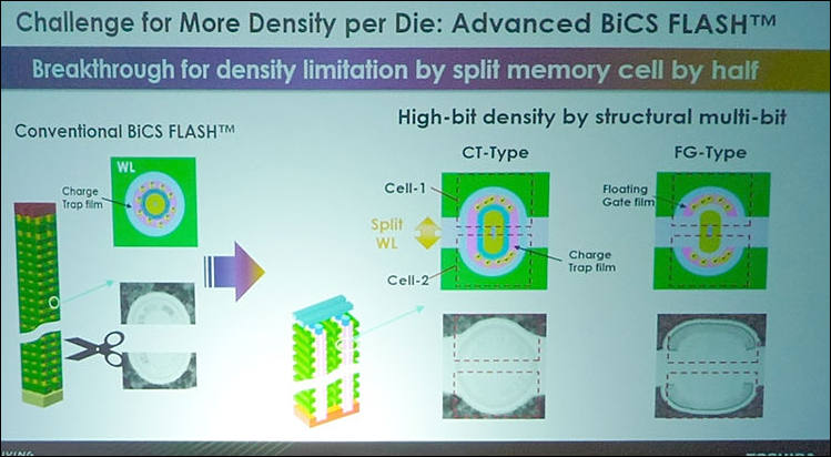
previously this had been proposed by Macronix
 sa9532.jpg749 x 412 - 56K
 sa9533.jpg781 x 383 - 54K
 -
Another Adata SU630 writing speed benchmark
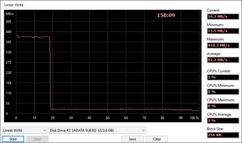
yes, it is slower than USB 2,0 old flash drives.
 sa9720.jpg800 x 471 - 60K
 -
Toshiba prepares PLC
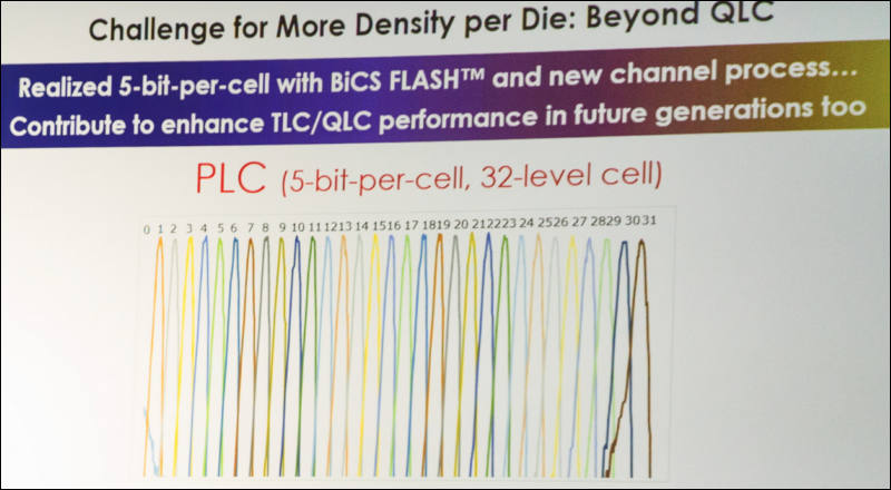
The company started research into Penta-level cell (PLC) NAND flash and verified working five-bit per cell NAND by modifying its current QLC NAND. The new flash provides more density with the ability to store five bits per cell, rather than just four in current QLC. But, to do this, the cell needs to be capable of storing 32 distinct voltage levels, and SSD controllers need to read them back accurately. With so many voltage levels to read to and write at nano-scale, the new technology is very challenging.
120Gb entry SSDs will reach 5-8Mb/sec write performance of HDDs around 1994, and 256-512Gb will have sustained write speed around 10-18Mb/sec similar to HDDs of around 1998.
 sa9745.jpg800 x 454 - 63K
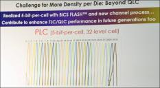 sa9747.jpg800 x 440 - 59K
 -
Tesla cars have NAND degradation that started to kill older cars
Lot of tesla cards started to have issues due to NAND chip degradation (too many writes and older age).
It is expected that almost all Test cars will have this issue later.
Note that tesla ask $1400 for replacement (replacement of chip is around $50).
 sa10455.jpg624 x 412 - 41K
 -
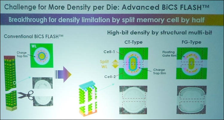
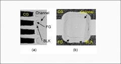
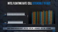
Kioxia Corporation today announced the development of the world’s first[1] three-dimensional (3D) semicircular split-gate flash memory cell structure “Twin BiCS FLASH” using specially designed semicircular Floating Gate (FG) cells. Twin BiCS FLASH achieves superior program slope and a larger program/erase window at a much smaller cell size compared to conventional circular Charge Trap (CT) cells. These attributes make this new cell design a promising candidate to surpass four bits per cell (QLC) for significantly higher memory density and fewer stacking layers. This technology was announced at the IEEE International Electron Devices Meeting (IEDM) held in San Francisco, CA on December 11th.
3D flash memory technology has achieved high bit density with low cost per bit by increasing the number of cell stacked layers as well as by implementing multilayer stack deposition and high aspect ratio etching. In recent years, as the number of cell layers exceeds 100, managing the trade-offs among etch profile control, size uniformity and productivity is becoming increasingly challenging. To overcome this problem, Kioxia developed a new semicircular cell design by splitting the gate electrode in the conventional circular cell to reduce cell size compared to the conventional circular cell, enabling higher-density memory at a lower number of cell layers.
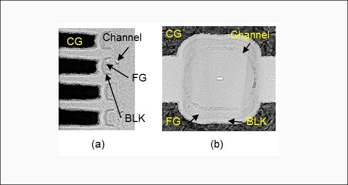
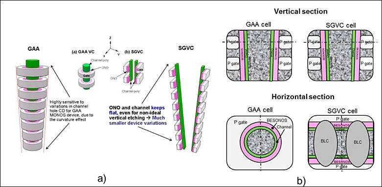
The circular control gate provides a larger program window with relaxed saturation problems when compared with a planar gate because of the curvature effect, where carrier injection through the tunnel dielectric is enhanced while electron leakage to the block (BLK) dielectric is lowered. In this split-gate cell design, the circular control gate is symmetrically divided into two semicircular gates to take advantage of the strong improvement in the program/erase dynamics. As shown in Fig. 1, the conductive storage layer is employed for high charge trapping efficiency in conjunction with the high-k BLK dielectrics, achieving high coupling ratio to gain program window as well as reduced electron leakage from the FG, thus relieving the saturation issue. The experimental program/erase characteristics in Fig. 2 reveal that the semicircular FG cells with the high-k-based BLK exhibit significant gains in the program slope and program/erase window over the larger-sized circular CT cells. The semicircular FG cells, having superior program/erase characteristics, are expected to attain comparably tight QLC Vt distributions at small cell size. Further, integration of low-trap Si channel makes possible more than four bits/cell, e.g., Penta-Level Cell (PLC) as shown in Fig. 3. These results confirm that semicircular FG cells are a viable option to pursue higher bit density.
Going forward, Kioxia’s research and development efforts aimed at innovation in flash memory will include continuing Twin BiCS FLASH development and seeking its practical applications. At IEDM 2019, Kioxia also announced six other papers highlighting the company’s intensive R&D activities in the area of flash memory.
 sa11479.jpg678 x 361 - 30K
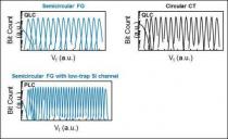 sa11480.jpg481 x 293 - 29K
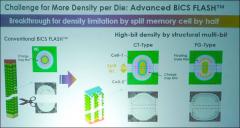 sa11481.jpg749 x 400 - 50K
 -
SK Hynix has unveiled its PCIe NVMe consumer SSD series. The drives are built with SK Hynix' 128-layer 4D NAND flash, just six months after the company announced mass production of its 128-layer 1Tb NAND chips.
"SK Hynix will begin the mass-production of its Terabyte-level high-performance NAND solution based on the 128-layer 4D NAND, and 1Znm DRAM in 2020," said the company in a statement.
-
New Xbox and Sony gaming consoles can be using cheapest QLC memory
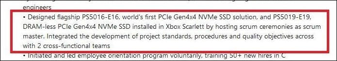
And very cheap Phison E19 controller
All will be soldered on main board and very hard to repair.
 sa11990.jpg695 x 127 - 28K
 -
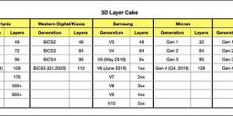
More layers ahead
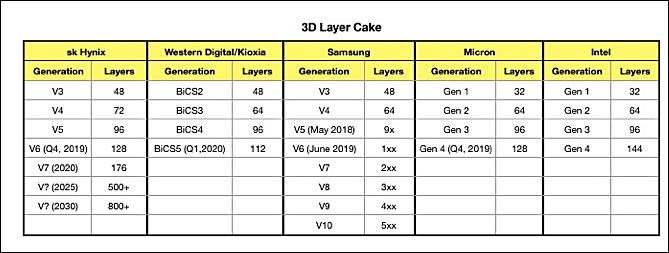
Western Digital and Kioxia (former Toshiba division) started making BiCS5 NAND with 112 layers.
 sa12041.jpg669 x 253 - 40K
 -
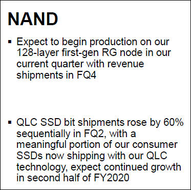
Intel's memory and storage group produced Intel QLC 3D NAND solid-state drive (SSD) number 10 million based upon the QLC NAND die built in Dalian, China. Production began in late 2018, and this milestone establishes QLC (quadruple-level cell memory) as a mainstream technology for high-capacity drives.
Dream of big companies.
Note that all consumers SSDs already are being made horribly wrong without capacitors enough to finish current operation (version for datacenters and good servers always have such!).
-
The spread of the coronavirus pandemic has dragged down considerably shipments for most end products in the first quarter of 2020, and can lead to cut of NAND flash bit output this year to about 30%.


Howdy, Stranger!
It looks like you're new here. If you want to get involved, click one of these buttons!
Categories
- Topics List23,992
- Blog5,725
- General and News1,354
- Hacks and Patches1,153
- ↳ Top Settings33
- ↳ Beginners256
- ↳ Archives402
- ↳ Hacks News and Development56
- Cameras2,367
- ↳ Panasonic995
- ↳ Canon118
- ↳ Sony156
- ↳ Nikon96
- ↳ Pentax and Samsung70
- ↳ Olympus and Fujifilm101
- ↳ Compacts and Camcorders300
- ↳ Smartphones for video97
- ↳ Pro Video Cameras191
- ↳ BlackMagic and other raw cameras116
- Skill1,960
- ↳ Business and distribution66
- ↳ Preparation, scripts and legal38
- ↳ Art149
- ↳ Import, Convert, Exporting291
- ↳ Editors191
- ↳ Effects and stunts115
- ↳ Color grading197
- ↳ Sound and Music280
- ↳ Lighting96
- ↳ Software and storage tips266
- Gear5,420
- ↳ Filters, Adapters, Matte boxes344
- ↳ Lenses1,582
- ↳ Follow focus and gears93
- ↳ Sound499
- ↳ Lighting gear314
- ↳ Camera movement230
- ↳ Gimbals and copters302
- ↳ Rigs and related stuff273
- ↳ Power solutions83
- ↳ Monitors and viewfinders340
- ↳ Tripods and fluid heads139
- ↳ Storage286
- ↳ Computers and studio gear560
- ↳ VR and 3D248
- Showcase1,859
- Marketplace2,834
- Offtopic1,320
Tags in Topic
- ssd 15


