It allows to keep PV going, with more focus towards AI, but keeping be one of the few truly independent places.
-
The breakthrough chip squeezes 50 billion transistors into area of 150 square millimeters. That puts its transistor density at just over 330 million transistors per square millimeter which is about 94% greater than the 5nm chips currently on the market (including Apple’s M1 and Huawei’s Kirin 9000 processors).
It’s also 14% greater than the upcoming chips based on TSMC’s 3nm process, which are due to start shipping some time next year.
IBM claims that the performance and efficiency gains over 7nm are substantial. When computational muscle is the top priority, its 2nm performs 45% better. When extended battery life is more important, IBM’s 2nm is capable of delivering performance on par with a 7nm chip while using about 75% less power.
Main purpose for this PR is to take blame from the industry, as chip manufacturers stole tens of billions of dollars during last months, they are also among main sponsors of crypto scam.
-
IBM’s new 2nm chip features about 333 million transistors per square millimeter (MTr/mm2). For comparison, TSMC’s most advanced chips, built using its 5nm process, feature about 173 million transistors per square millimeter (MTr/mm2), while Samsung’s 5nm chips feature about 127 MTr/mm2.
Note that it is fake info, as companies mention that they mean some abstract transistors, not real ones you can use in CPU logic, for example, where you need proper heat management, interference, more metal layers and so on.
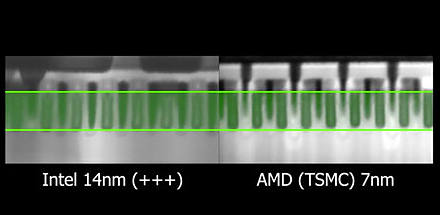
5nm is also utter marketing, real progress stopped at around 20-22nm, after this 14nm could shrink only certain features, "7nm" by TSMC being 12-14nm in reality even for such features, and 5nm being 7nm on steroids where focus was on SRAM, leaks and similar parts.
Now back to 2nm fakes, if we use numbers provided 173 millions must have turned into 1084 billions (2.5x2.5 = 6.25 times), but in reality it is not even 2 times.
Size of key features is reduced 40% tops (173×(1,4×1,4) = 339,08), but transistors can't be made smaller, so now all this went in rising vertical part (whole progress since 22nm had been vertical already, even most 22nm chips used this a lot).
-
Marketing at its best:

 sa17228.jpg391 x 234 - 13K
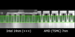 sa17229.jpg440 x 215 - 14K


Howdy, Stranger!
It looks like you're new here. If you want to get involved, click one of these buttons!
Categories
- Topics List23,991
- Blog5,725
- General and News1,353
- Hacks and Patches1,153
- ↳ Top Settings33
- ↳ Beginners256
- ↳ Archives402
- ↳ Hacks News and Development56
- Cameras2,367
- ↳ Panasonic995
- ↳ Canon118
- ↳ Sony156
- ↳ Nikon96
- ↳ Pentax and Samsung70
- ↳ Olympus and Fujifilm101
- ↳ Compacts and Camcorders300
- ↳ Smartphones for video97
- ↳ Pro Video Cameras191
- ↳ BlackMagic and other raw cameras116
- Skill1,960
- ↳ Business and distribution66
- ↳ Preparation, scripts and legal38
- ↳ Art149
- ↳ Import, Convert, Exporting291
- ↳ Editors191
- ↳ Effects and stunts115
- ↳ Color grading197
- ↳ Sound and Music280
- ↳ Lighting96
- ↳ Software and storage tips266
- Gear5,420
- ↳ Filters, Adapters, Matte boxes344
- ↳ Lenses1,582
- ↳ Follow focus and gears93
- ↳ Sound499
- ↳ Lighting gear314
- ↳ Camera movement230
- ↳ Gimbals and copters302
- ↳ Rigs and related stuff273
- ↳ Power solutions83
- ↳ Monitors and viewfinders340
- ↳ Tripods and fluid heads139
- ↳ Storage286
- ↳ Computers and studio gear560
- ↳ VR and 3D248
- Showcase1,859
- Marketplace2,834
- Offtopic1,320


