It allows to keep PV going, with more focus towards AI, but keeping be one of the few truly independent places.
-
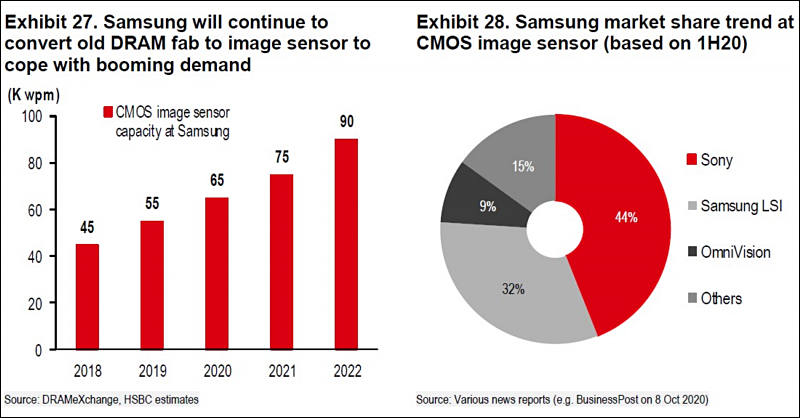
Manufacturing process technology is similar to DRAM, so CIS expansion is usually done in Samsung by using old used DRAM equipment
This is main Sony reason of joining cartel, as Japanese silicone capabilities are quickly deteriorating and Samsung is huge DRAM manufacturer thst can make sensors very cheap due to saving on equipment (and Sony can't).
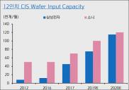
Samsung CIS production capacity is now close to Sony and will soon significantly surpass Sony.

Sony perfectly know huge dangers of much bigger company who has source of almost free equipment.
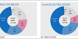
- Samsung's Non-Memory Division revenue breakdown by product: Foundry 41%, CIS 19%, DDI 15%, AP 23%
- Cumulative growth since 2010: Foundry + 1,053%, CIS +457%, DDI 60%, AP +229%
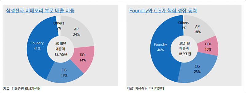
- Cumulative growth forecast for 2018-2021: Foundry +63%, CIS +87%, DDI -3%, AP +14%
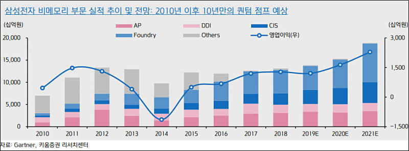
Via http://www.paxnet.co.kr/WWW/data/researchCenter/attach/20190522132833147.pdf
 sa11359.jpg705 x 497 - 43K
 sa11360.jpg707 x 543 - 56K
 sa11357.jpg800 x 303 - 34K
 sa11358.jpg800 x 297 - 43K
 -
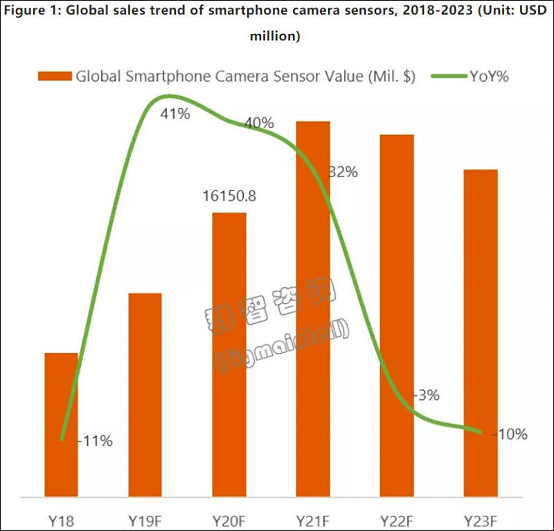
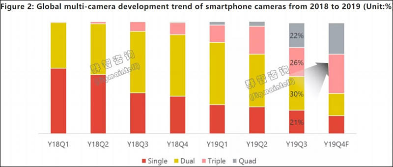
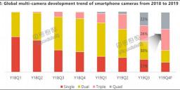
The upgrade of 48M and above pixels accelerated, with a market share of about 9% in the third quarter. Among them, Sony accounts for approximately 41%, Samsung accounts for approximately 56%, and OV accounts for approximately 3%. Due to the accelerated replacement of 48M and the insufficient production capacity of high-resolution camera sensor wafers, Sigmaintell expects supply shortages from Q4 to Q1 2019. According to Sigmaintell data , global shipments of 48M camera sensors will exceed 450 million units in 2020.
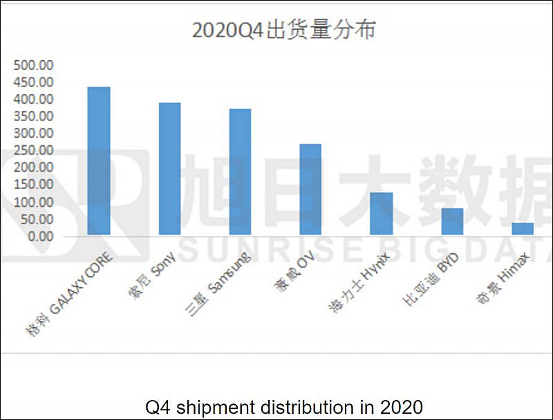
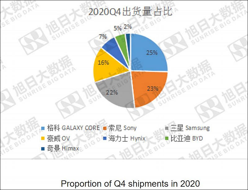
For modern mobile sensors cartel now control 97% of the market.
Some predictions:
 sa11400.jpg800 x 767 - 64K
 sa11399.jpg800 x 340 - 37K
 -
And now this have this
Sony Corp. is working around the clock to manufacture its in-demand image sensors, but even a 24-hour operation hasn’t been enough.
For the second straight year, the Japanese company will run its chip factories constantly through the holidays to try and keep up with demand for sensors used in mobile phone cameras, according to Terushi Shimizu, the head of Sony’s semiconductor unit.
“Judging by the way things are going, even after all that investment in expanding capacity, it might still not be enough,” Shimizu said in an interview at the Tokyo headquarters. “We are having to apologize to customers because we just can’t make enough.”
Something is up here, Sony seems to be very afraid by latest Samsung moves and want at all costs assure their clients that total demand is astonishing.
-
Samsung Electronics will invest in expanding foundry facilities for CMOS image sensors (CISs).
The company is drawing up a detailed plan to convert part of its production lines for DRAMs in Hwaseong, Gyeonggi Province to CIS lines.
In 2018, the company converted part of its DRAM line 11, which is based on 300-mm (12-inch) wafers, to image sensor production line S4.
This time, the company is expected to reduce capacity at DRAM line 13 in Hwasung for CIS conversion.
A DRAM production line can be easily converted into an image sensor line because their processes are 80 percent identical. Some of the lithography, chemical vapor deposition (CVD), etching, and testing equipment used for DRAM production can be used for image sensor production.
Industry experts say that mass-production of image sensors at the converted lines can begin within this year after new equipment is installed, tested and stabilized. They predict that Samsung will spend at least one trillion won on this conversion project, although it requires less money than investment in fresh production facilities.
We can see first small breakups of cartel as early as Seprember-October. And major one in the next year.
-
Samsung has recently signed a contract for UMC to manufacture Samsung’s image sensors in Taiwan.
As a part of the deal, Samsung is selling about 400 units of fab equipment to UMC to be installed at USMC's P6 fab at Nanke and used in the sensor manufacturing. UMC expects to produce 27,000 28nm wafers per month at the fab starting sometime in 2023.
Interesting deal.
Howdy, Stranger!
It looks like you're new here. If you want to get involved, click one of these buttons!
Categories
- Topics List23,990
- Blog5,725
- General and News1,353
- Hacks and Patches1,153
- ↳ Top Settings33
- ↳ Beginners256
- ↳ Archives402
- ↳ Hacks News and Development56
- Cameras2,367
- ↳ Panasonic995
- ↳ Canon118
- ↳ Sony156
- ↳ Nikon96
- ↳ Pentax and Samsung70
- ↳ Olympus and Fujifilm101
- ↳ Compacts and Camcorders300
- ↳ Smartphones for video97
- ↳ Pro Video Cameras191
- ↳ BlackMagic and other raw cameras116
- Skill1,960
- ↳ Business and distribution66
- ↳ Preparation, scripts and legal38
- ↳ Art149
- ↳ Import, Convert, Exporting291
- ↳ Editors191
- ↳ Effects and stunts115
- ↳ Color grading197
- ↳ Sound and Music280
- ↳ Lighting96
- ↳ Software and storage tips266
- Gear5,420
- ↳ Filters, Adapters, Matte boxes344
- ↳ Lenses1,582
- ↳ Follow focus and gears93
- ↳ Sound499
- ↳ Lighting gear314
- ↳ Camera movement230
- ↳ Gimbals and copters302
- ↳ Rigs and related stuff273
- ↳ Power solutions83
- ↳ Monitors and viewfinders340
- ↳ Tripods and fluid heads139
- ↳ Storage286
- ↳ Computers and studio gear560
- ↳ VR and 3D248
- Showcase1,859
- Marketplace2,834
- Offtopic1,319


