-
 sa13063.jpg715 x 822 - 111K
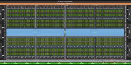 sa13064.jpg800 x 391 - 102K
 sa13065.jpg722 x 960 - 189K
 -
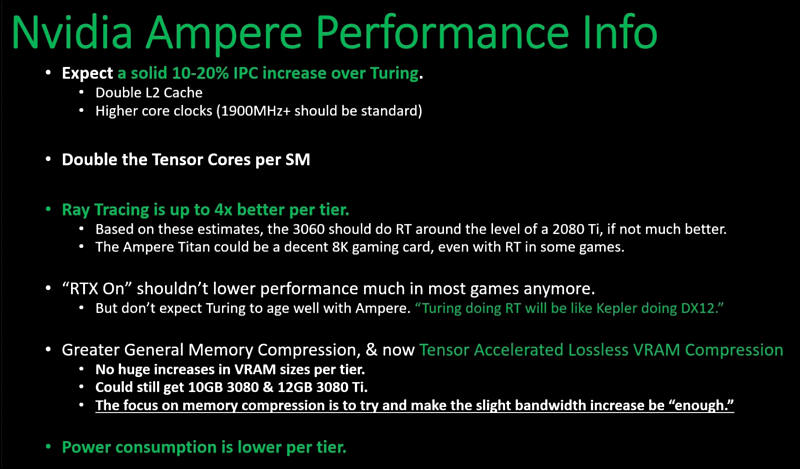
Ampere expected to offer a 10-20% IPC increase, 4x the ray tracing performance, and clocks that can be easily pushed to 2 GHz.
 sa13008.jpg800 x 514 - 67K
 sa13009.jpg800 x 469 - 64K
 -
Graphics chip maker NVIDIA in May will release a new generation of 7nm graphics chip products, produced by TSMC.
It is strong rumors that delay had been caused by catastrophic Samsung 7nm process issues.
-
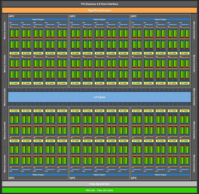
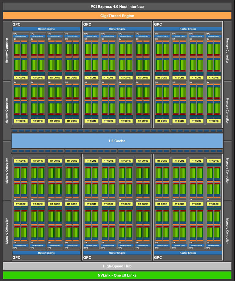
GA100 will support up to 8,192 CUDA cores. Additionally, the GA100 will feature up to 48 GB of HBM2e VRAM and a TDP of 300 W, while its core can apparently clock up to 2.2 GHz.
GA102 will support 5,376 CUDA cores and 12 GB of VRAM. The GA102 will apparently feature 7 graphics processing clusters (GPCs) too, all the while achieving 40% better performance than the RTX 2080 Ti.
-
Some first leaks
- GA103: 60 blocks, 3480 CUDA cores, 320-bit video memory bus, 10 or 20GB GDDR6 video memory capacity.
- GA104: 48 blocks, 3072 CUDA cores, 256-bit video memory bus, 8 or 16GB GDDR6 video memory capacity.
- 7nm architecture
- Card names will be RTX 3080、RTX 3070
- RTX 3080 Ti and Titan will have GP102 chip.
-
According to Chris Caso via HKEPC, an analyst at Raymond James, NVIDIA is aiming to unveil high-end Ampere GPUs at Computex 2020. Hosted in Taipei from June 2 through June 6, Computex 2020 will probably mark the arrival on the RTX 3070, RTX 3080 and RTX 3080 Ti, with midrange cards appearing in Q3.
We may see NVIDIA unveil the Ampere architecture early than June though, albeit not as consumer GPUs. Instead, Caso claims that the company will use GTC 2020 in March to demonstrate Ampere-based Tesla GPUs.
I think it won't happen in 2020. And instead we'll see anther rehash of existing cards with memory upgrades.
-
Nvidia made bet on Samsung 5nm EUV process

Now it is absolutely not ready for anything.
Even in 2020 it is expected only small test manufacturing with level of defects reaching 70-80%.
We can see Nvidia chips delays as much as 2 years (original release must had been late 2019), and they can see light in 2021-2022.
Rumors are that original plans had been to use 7nm by Samsung, but results had been so horrible that Nvidia decided to wait for mythical 5nm EUV.
 sa10801.jpg800 x 477 - 44K
 -
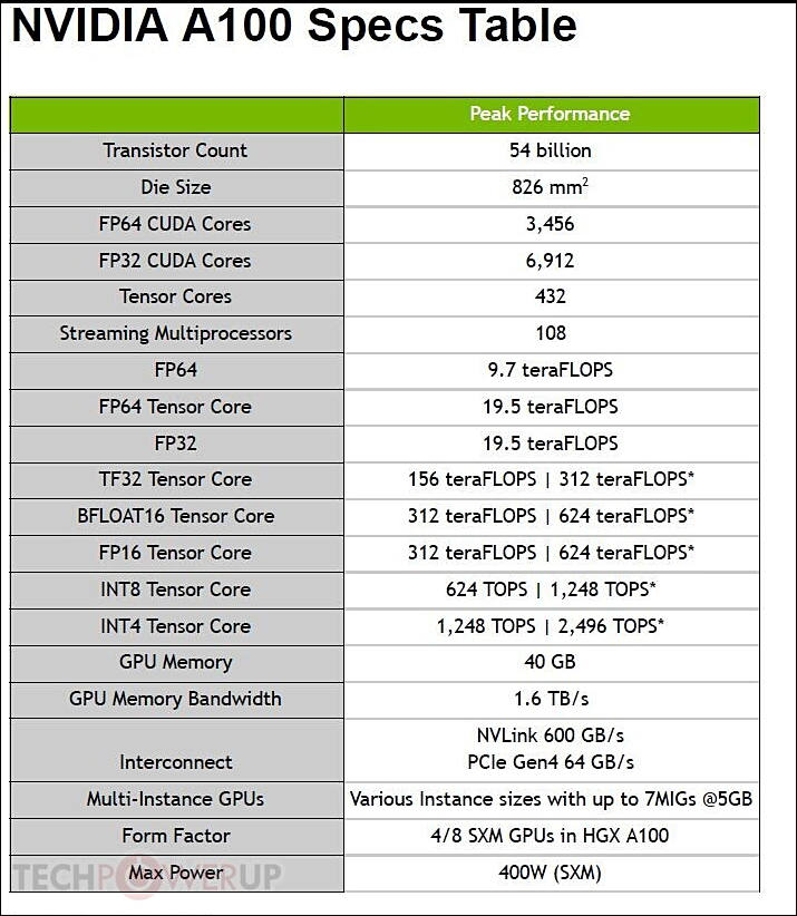
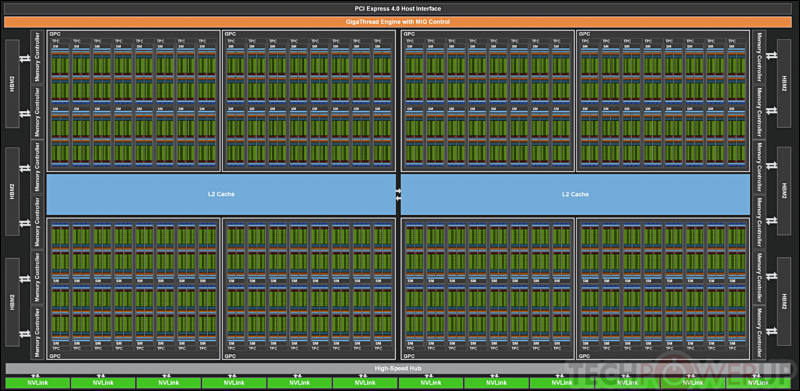
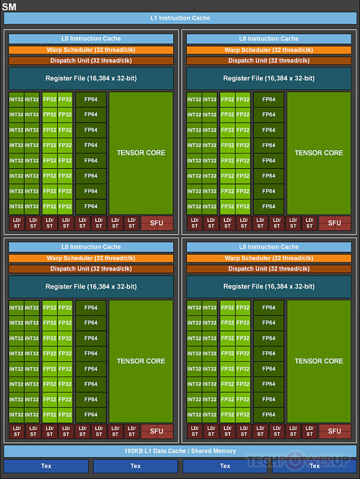
GA100 largest chip
- 800mm2 die
- 55 Billion transistors
- 2304 Gbps bandwidth speed
- 6 HMB memory stacks
GA101 half performance chip
- 400mm2 die
- Around 30 Billion transistors
- Half memory speed
- 3 HMB memory stacks
- Cancelled


Howdy, Stranger!
It looks like you're new here. If you want to get involved, click one of these buttons!
Categories
- Topics List23,990
- Blog5,725
- General and News1,353
- Hacks and Patches1,153
- ↳ Top Settings33
- ↳ Beginners256
- ↳ Archives402
- ↳ Hacks News and Development56
- Cameras2,366
- ↳ Panasonic995
- ↳ Canon118
- ↳ Sony156
- ↳ Nikon96
- ↳ Pentax and Samsung70
- ↳ Olympus and Fujifilm100
- ↳ Compacts and Camcorders300
- ↳ Smartphones for video97
- ↳ Pro Video Cameras191
- ↳ BlackMagic and other raw cameras116
- Skill1,960
- ↳ Business and distribution66
- ↳ Preparation, scripts and legal38
- ↳ Art149
- ↳ Import, Convert, Exporting291
- ↳ Editors191
- ↳ Effects and stunts115
- ↳ Color grading197
- ↳ Sound and Music280
- ↳ Lighting96
- ↳ Software and storage tips266
- Gear5,420
- ↳ Filters, Adapters, Matte boxes344
- ↳ Lenses1,582
- ↳ Follow focus and gears93
- ↳ Sound499
- ↳ Lighting gear314
- ↳ Camera movement230
- ↳ Gimbals and copters302
- ↳ Rigs and related stuff273
- ↳ Power solutions83
- ↳ Monitors and viewfinders340
- ↳ Tripods and fluid heads139
- ↳ Storage286
- ↳ Computers and studio gear560
- ↳ VR and 3D248
- Showcase1,859
- Marketplace2,834
- Offtopic1,320


