-
Yield rates for Taiwan Semiconductor Manufacturing Company's (TSMC) 10nm process technology have still been too low to boost the process to economies of scale, said the sources.
Yield rates for Samsung's 10nm process technology have been low affecting production for its own Exynos 8895 and Qualcomm's Snapdragon 835 chips, the sources revealed. The unsatisfactory 10nm yield rates have already pushed back Samsung's schedule to launch the next-generation Galaxy S8 smartphone.
-
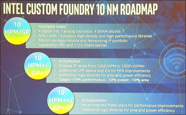
Intel now propose that their 10nm is the real deal, else are all fakes

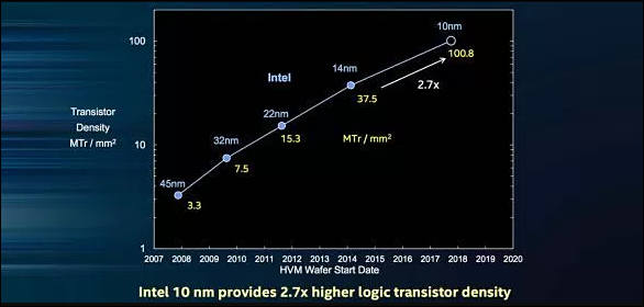
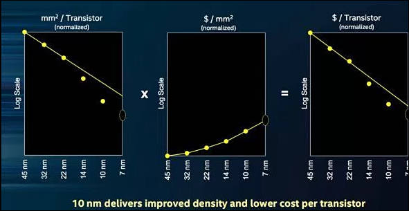
 sample1039.jpg678 x 388 - 40K
 sample1040.jpg586 x 280 - 21K
 sample1041.jpg591 x 305 - 27K
 -
 sample1086.jpg750 x 977 - 154K
 -
PR machine broke
Intel has evolved its event portfolio and decided to retire the IDF program moving forward. Thank you for nearly 20 great years with the Intel Developer Forum! Intel has a number of resources available on intel.com, including a Resource and Design Center with documentation, software, and tools for designers, engineers, and developers. As always, our customers, partners, and developers should reach out to their Intel representative with questions.
Intel cancelled both IDF events.
-
Optimism for investors
Taiwan Semiconductor Manufacturing Company (TSMC) is set to move its 7nm process technology to volume production in 2018, an improved version of the 7nm process using extreme ultraviolet (EUV) will be ready for volume production a year later, according to company co-CEO CC Wei.
TSMC's manufacturing technologies are offered to target four main applications - mobile, high-performance computing, automotive and IoT, Wei indicated. TSMC has already moved its 10nm process technology focusing mainly on mobile devices to volume production.
Now actually AMD could not meet demand due to simple fact that unable to produce enough 14nm chips.
Huge delays with 835 chip and total shortage of it also come from similar issue.
-
Intel forced to stay on 14nm for longer
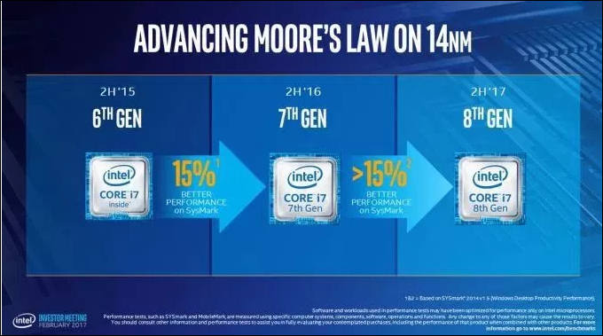
And usual lie about 15% that will more like 0-3%
 sample357.jpg680 x 379 - 46K
 -
Optimism is fascinating:
TSMC disclosed previously its 7nm process will be ready for risk production in the second quarter of 2017, followed by volume production in 2018. The foundry has secured 12 design tape-outs for the process.
Samsung has unveiled plans to enter volume production of 7nm chips in 2018.
Globalfoundries recently announced the availability of its 7LP (7nm leading-performance) FinFET semiconductor technology, and expects the first customer products based on the technology to launch in the first half of 2018 with volume production ramping in the second half of 2018.
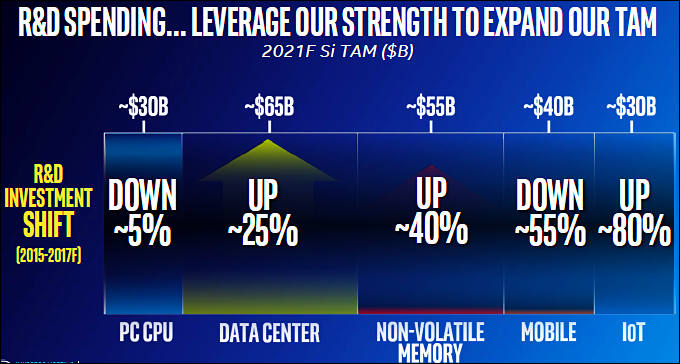
Of course things will shift a lot from this proposed data, at least for anything besides PGA and memory.
-
IBMs 5nm tech
-
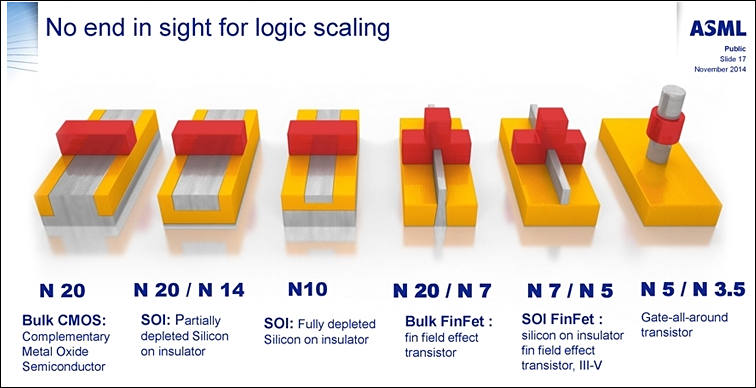
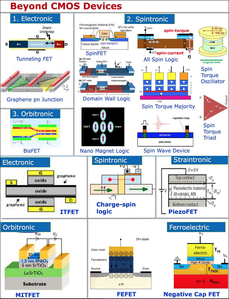
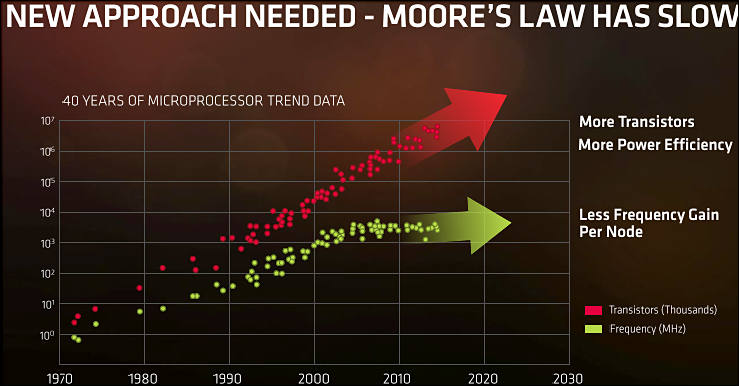
Transistors & The End of Moore's Law
-
Nvidia is worried
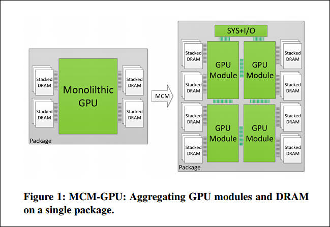
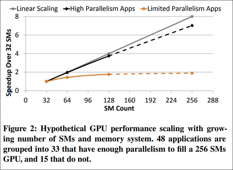
Unfortunately, despite the application performance scalability with the increasing number of SMs, the observed performance gains are unrealizable with a monolithic single-die GPU design. This is because the slowdown in transistor scaling eventually limits the number of SMs that can be integrated onto a given die area. Additionally, conventional photolithography technology limits the maximum possible reticle size and hence the maximum possible die size. For example, ≈ 800mm2 is expected to be the maximum possible die size that can be manufactured. For the purpose of this paper we assume that GPUs with greater than 128 SMs are not manufacturable on a monolithic die.
 sample804.jpg649 x 447 - 47K
 sample805.jpg800 x 584 - 81K
 -
And even revised plan must be revised again and again
 sample904.jpg746 x 492 - 89K
 -
Intel Cannon Lake architecture will contain only small mobile CPUs.
Intel now is unable to produce 10nm big complex chips without very low yield rate.
Si it'll be around 2019 as you could see any 10nm desktop CPUs.
-
EUV is last hope now
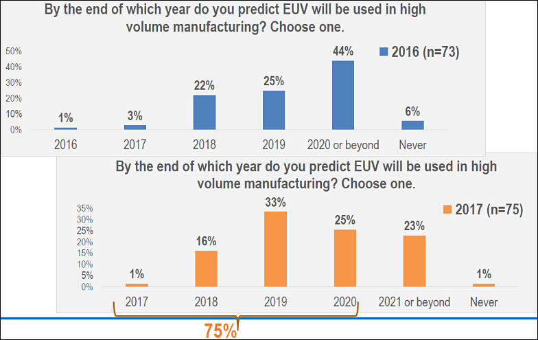
Firms and bosses did not wanted to use it, but now have no other option
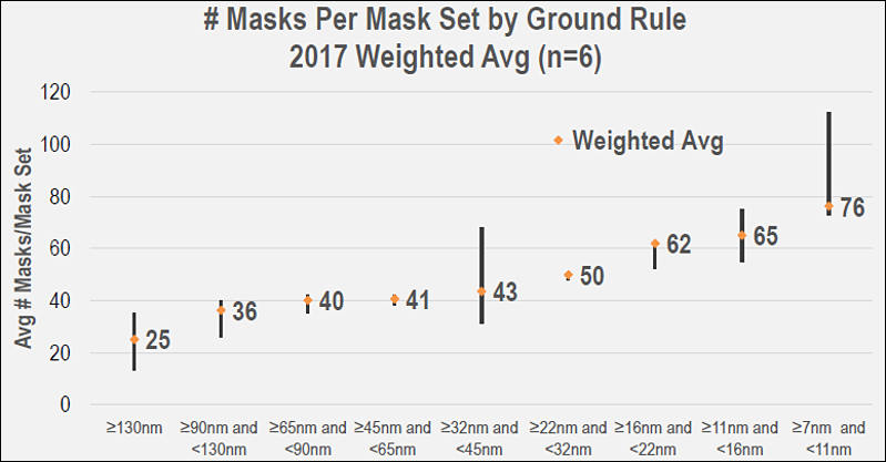
And this is why - masks count became too big.
 s841.jpg784 x 495 - 60K
 s842.jpg799 x 417 - 44K
 -
Nvidia founder and CEO Jensen Huang said that with the emergence of GPU computing following the decline of the CPU era, Moore's Law has come to an end. Huang made the statement when delivering a keynote speech at the GPU Technology Conference (GTC) China 2017, held on September 26 in Beijing.
Remarks came in sharp contrast to an earlier statement that Moore's Law will not fail, as issued by Intel at its Technology and Manufacturing Day held also in Beijing, on September 19, when the company provided updates for its 10nm process.
End for GPUs will be even harder and sharper.
-
Still no EUV in DRAM
The industry was previously anticipated to transition to EUV litho technology beyond 20nm, but the high cost of EUV litho tools has discouraged Samsung and other DRAM chipmakers from pursuing the technology for their 1xnm manufacturing lines, said the sources. The DRAM industry will continue to stick with 193nm immersion lithography with multiple patterning for their 1ynm, and possibly 1znm lines for some of the players.
-
Intel afraid of EUV
A race is on to qualify advanced semiconductor process technologies using extreme ultraviolet (EUV) lithography, but Intel is said to be sitting on the sidelines.
Samsung and TSMC are racing to announce some level of manufacturing with EUV next year. But Intel is said not to be ordering materials needed for EUV at the same rate, according to one source that asked not to be named.
-
Samsung Electronics 8nm FinFET process
Samsung's new 8LPP process provides up to 10% lower power consumption with up to 10% area reduction from 10LPP through narrower metal pitch. 8LPP will provide differentiated benefits for applications including mobile, cryptocurrency and network/server, and is expected to be applied to many other high-performance applications, the company said.
"8LPP will have a fast ramp since it uses proven 10nm process technology while providing better performance and scalability than current 10nm-based products."
-
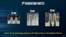
Intel and Globalfoundries will describe their 10nm and 7nm process nodes, respectively at the International Electron Devices Meeting (IEDM) in December. The event also will host papers pointing to new directions in memories, medical and flexible electronics and transistors beyond today’s FinFETs.
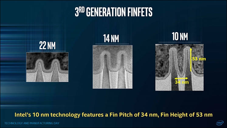
Intel will discuss several aspects of its 10nm node first unveiled in March. It sports FinFETs with a 7nm fin width at a 34nm pitch and a 46nm fin height made using self-aligned quadruple patterning. A 204 Mbit SRAM made in the process packs separate high-density, low voltage and high-performance cells that measure from 0.0312µm2 to 0.0441µm2.
 sa142.jpg747 x 421 - 44K
 sa143.jpg756 x 388 - 52K
 -
More surprises
Moore's Law has become invalid for a while, as the time needed for the transistor density to double is no longer 18-24 months, Morris Chang, chairman of Taiwan Semiconductor Manufacturing Company (TSMC) said.
TSMC will continue to increase transistor densities in the coming eight years, but will see a major challenge in 2025.
ASML CEO Peter Wennick said at the same forum that his company has worked out its technology development plans through 2030. It might be technologically feasible for ASML to carry out the plans, but the economic feasibility of the plans would meet with challenges before 2030.
-
Poor Moore law, they constantly want to dig up the grave and get out the corpse
The Moore's Law that sets the pace of the semiconductor development can last two more generations, as the process technology may hit bottlenecks after advancing to 3nm node from the existing 7nm and future 5nm nodes, Tsai Ming-kai, chairman of Taiwan's leading IC designer MediaTek, has said.
-
Samsung Electronics secured new customers from the U.S. and China for its 7-nano foundry business. This indicates that it succeeded in making a counterattack after it lost rights to produce Qualcomm’s 7-nano chips to TSMC. It is heard that it is finalizing a negotiation with Hwasung-si regarding construction of new 7-nano plant and finalize administrative procedures early December at the earliest. Positive forecast is seen for its 7-nano foundry business.
Qualcomm and Broadcom are designing next-generation chips through TSMC’s7-nano PDK. TSMC is planning to produce 7-nano chips by using normal steppers repeatedly. Due to this reason, many customers including Qualcomm decided to mass-produce their first 7-nano chips through TSMC.
It is expected that Samsung Electronics will be slightly late in commercializing 7-nano process than TSMC. However it has been emphasizing that its 7-nano process that is applied with EUV (Extreme Ultraviolet) photolithography technology is truly the next-generation process from all aspects such as area, performance, and amount of electricity consumption.
So, finally they are forced to do EUV.
-
As it is too soon for 8nm, second gen 10nm is presented
Samsung announced that its Foundry Business has commenced mass production of System-on-Chip (SoC) products built on its second generation 10-nanometer (nm) FinFET process technology, 10LPP (Low Power Plus).
10LPP process technology allows up to 10-percent higher performance or 15-percent lower power consumption compared to its first generation 10nm process technology, 10LPE (Low Power Early). As this process is derived from the already proven 10LPE technology, it offers competitive advantages by greatly reducing turn-around time from development to mass production and by providing significantly higher initial manufacturing yield.


Howdy, Stranger!
It looks like you're new here. If you want to get involved, click one of these buttons!
Categories
- Topics List23,992
- Blog5,725
- General and News1,354
- Hacks and Patches1,153
- ↳ Top Settings33
- ↳ Beginners256
- ↳ Archives402
- ↳ Hacks News and Development56
- Cameras2,367
- ↳ Panasonic995
- ↳ Canon118
- ↳ Sony156
- ↳ Nikon96
- ↳ Pentax and Samsung70
- ↳ Olympus and Fujifilm101
- ↳ Compacts and Camcorders300
- ↳ Smartphones for video97
- ↳ Pro Video Cameras191
- ↳ BlackMagic and other raw cameras116
- Skill1,960
- ↳ Business and distribution66
- ↳ Preparation, scripts and legal38
- ↳ Art149
- ↳ Import, Convert, Exporting291
- ↳ Editors191
- ↳ Effects and stunts115
- ↳ Color grading197
- ↳ Sound and Music280
- ↳ Lighting96
- ↳ Software and storage tips266
- Gear5,420
- ↳ Filters, Adapters, Matte boxes344
- ↳ Lenses1,582
- ↳ Follow focus and gears93
- ↳ Sound499
- ↳ Lighting gear314
- ↳ Camera movement230
- ↳ Gimbals and copters302
- ↳ Rigs and related stuff273
- ↳ Power solutions83
- ↳ Monitors and viewfinders340
- ↳ Tripods and fluid heads139
- ↳ Storage286
- ↳ Computers and studio gear560
- ↳ VR and 3D248
- Showcase1,859
- Marketplace2,834
- Offtopic1,320


