-
Development and production costs of modern cameras are huge. And they will become much worse.
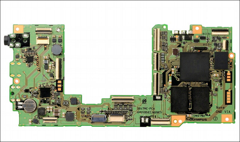
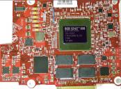
Check image of E-M1 main board above. Usually biggest chips in modern cameras are as follows : main LSI chip, one or more RAM chips, flash chips.
In some cases, like in some modern Panasonic cameras it can be something that looks like one chip only - with main LSI located directly below custom chip that contains both flash and RAM.
Development of all of the chips mentioned is very complex and costly task. But they have one core difference - you can get modern mobile RAM (DDR2 or DDR3 usually) chips, same is true for flash. But if you are serious company you develop your own main LSI. Sometimes it is join efforts, for example Nikon use Fujitsu FR image LSI as core for further modifications. Join development allow to save costs, but usually means that any problem of the partner prevents adding important features (like Fujitsu FR issues with video until last generation).
Another core difference between this chips is the process that is used to manufacture them. RAM and Flash usually are at forefront of progress, as they are simpler chips and development costs are lower with better yields and ability to compensate increased costs with instantly visible increased capacity.
For LSI is much more difficult. Latest Fujitsu based LSI (like in Nikon) are still 65nm, as far as I know many other LSI are also in same or slightly smaller process. This is in the times were most mobile CPUs went 28nm. Why it is so?
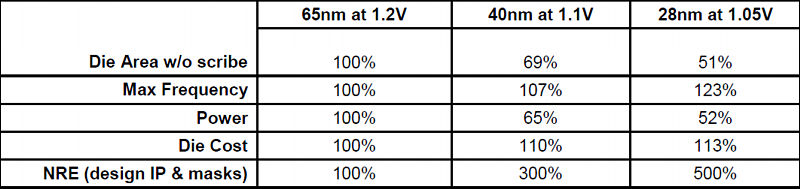
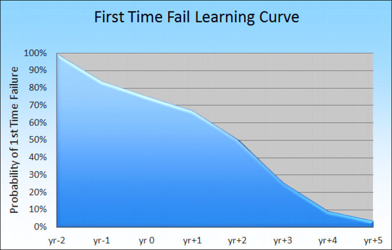
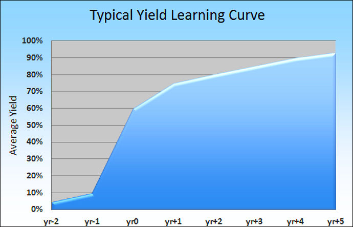
Answer here is simple - development costs and ability to return investments. You can check table below:
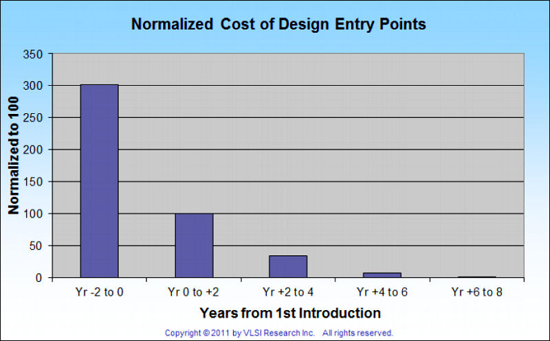
Further it become even worse:
Companies try to overcome this with existing process optimizations like SuVolta ones.
the MB86S22AA Milbeaut image processing chip — the DDC tech can cut power consumption by 30 percent, but it can still have twice the processing performance of comparable chips. Fujitsu and SuVolta have been working together since the Summer of 2011.
In case of new process costs rise even more due to problems associated with initial stages of production.
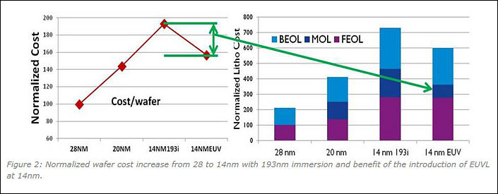
Charts from http://m.eet.com/media/1160433/sv_mw_b_120601_technology%20extension%20oped_revm.pdf
How big are this costs?
Non-recurring engineering costs estimates for 28nm complex image LSI are about $29 millions of dollars.In case of more iterations of development, producing more masks and modifications costs can be as high as $50 millions.
All this money must be returned from chip sales inside cameras. Millions of cameras.
Small companies usually have no chance to do it, so they use other solution - modern FPGA chips. We'll discuss in detail their specifics and development costs in next post.
So, as you see sharply declining sales of compact cameras do not start smile happily looking at your smartphone. Most of this cameras use same LSI as in big cameras, sometimes clocked down and with smaller amount of slower memory, but same chips. As otherwise it becomes impossible to be profitable.
Today all camera companies face complex problems:
- Necessity to move to 28nm (who did not do it already) and later to 14nm.
- Sharply rising development costs
- Declining overall cameras sales resulting in constant cuts and optimizations that have almost no effect.
- Steady or declining average camera prices (all companies went with idea to introduce premium cameras and design to rise the price)
In upcoming posts we'll touch FPGA development problems, 14nm costs comparisons, flash and ram issues, screens problems
-
OK, up to this point we've learned that the death of the compact camera market will have serious implications on the SLR/mirrorless market since increased development costs for the onboard logic (shared by cameras of all types) can't be recuperated via camera volume sales any longer. This may likely amount to the death of the consumer camera divisions of all current camera manufactures. The smaller ones might get bought up or go out of business, Canon and Nikon might transition to non-consumer markets like scientific, medical and industrial imaging and will likely keep very few expensive pro camera bodies in their product line-up. It would be the history of analog 35mm photography repeating itself, a market that had been saturated by the 90s before digital photography brought a massive comeback of consumer demand.
But why should this have implications for small scale, specialty manufacturers like Blackmagic? They are under no pressure of using more advanced (40nm or 28nm) chip technology since their firmware is much more simple and has to perform much less tasks. And as niche manufacturers living off a much smaller customer base, they're more likely to survive the imminent apocalypse of the consumer camera market.
-
But why should this have implications for small scale, specialty manufacturers like Blackmagic? They are under no pressure of using more advanced (40nm or 28nm) chip technology since their firmware is much more simple and has to perform much less tasks. And as niche manufacturers living off a much smaller customer base, they're more likely to survive the imminent apocalypse of the consumer camera market.
In fact, points above have direct implications on small manufacturers mostly. As you can't reduce non-recurring engineering costs much. And while they restrict features and capabilities they still mostly can't produce any complex custom chips.
Big manufacturers won't vanish, they'll be making development together. Btw, this year Panasonic signed similar to Nikon agreement with Fujitsu (but it won't just use their solutions, just join some engineering).
It'll be in next parts about costs of FPGA solutions (they are not good either) they try to use to mitigate problems. FPGA is also highly inefficient (read - bad battery life and cooling).
-
What about using newer ARM or Intel SOC to do the heavy lifting?
-
ARM to hot to handle on camera, FPGA is a programable chip but inefficient as vitaly said. The latest ARM octocore from samsung is a heat sink us it on galaxy S4 and it will burn your hand no joke.
As for black magic, they are in real trouble if they dont joint efforts with other company. As vitaly mentioned developing a concrete manufacturing process for any chip is really expensive, and transitioning even thr same fucking desing to a smaller manufacturing process is sometimes more expensive than its developement. Since lithography is very complex almost i could say is ART science stuff, since shrinking designs and make them work properly is a pain in the ass. As far as i know only a few know how to develop corectly a samller process, dont mention that the more little the nanometer the more prone to fail inside chip and current leak and bad yield.
Even intel has i think only 2 scientists living in israel that are the artists of making this process.
With no money, and this graphs its not good for BMCC
-
So far, the premise of this seems to be fundamentally flawed. Sure, development of custom chips is expensive and if BM tried to compete with partnered large imaging corporations on that level, they'd fail quickly. However, if they keep their focus on shooting raw, there's not a lot in their cameras that should require massive horsepower. All they need to do is manage to find a low power processor with enough horsepower to debayer the image for display and do things like focus peaking, etc.
Prores is a little trickier, but as long as someone has made a hardware encoder/decoder, they can just buy that too. If not, they could switch future cameras to another codec (DNxHD, Cineform) depending on which is available inexpensively in a dedicated chip.
That's also not to mention that the large complicated LSI in cameras from the likes of Canon, Nikon, etc. tends to have a lot more concerns than would be needed in a Black Magic camera. Their current cameras don't need to care about jpeg compression (with multiple levels of detail), high resolution stills, face recognition, mp4 compression, "art" filters, fancy exposure/metering modes, wifi, music slideshows, or any of a number of other things that other manufacturers are building into their LSI chips.
So yeah. Building chips is expensive. Black Magic should avoid having to do that. Instead, they can and should just continue their focus on integrating inexpensive components and not get too distracted with unnecessary features.
-
@eatstoomuchjam seems that you don't understand approach. LSI is part of the native design of a compact camera, eve if its raw only. Image prepossessing is on hell of a task, we are not even talking about compressing.
Debayering an image cant be made by "any chip" must be a dedicated one, since sensor has its own particular aproach and specs. Use any chip will be to you use a FPGA and try to make sensor debayering work, you will enter a huge amount of drawbacks on your options. Thats why LSI is made, for efficient workflow.
The problem is that the development of this integrated machines chips is expensive and i think a small company like BM cant afford in long term a proper integration in research and development in large scale for such chips.
Too expensive. I belive that the " problem " for delivery in their first production 2.5k was due to LSI problems than the "bad sensor yield" since their provider has good experience in lithography, and those cut down sensors are not that complex.
-
So yeah. Building chips is expensive. Black Magic should avoid having to do that. Instead, they can and should just continue their focus on integrating inexpensive components and not get too distracted with unnecessary features.
Black Magic should avoid having to do that. Instead, they can and should just continue their focus on integrating inexpensive components and not get too distracted with unnecessary features.
I'll touch features and necessary properties LSI or FPGA qualities. Also, if you think that custom development and design for integration of some more general thing is cheap - you are wrong. Camera system LSI has big advantages from all points - from ready to implement design guidelines, to very handy interfaces and implementations, to cheap and simple power solutions required to run such chip.
-
One good example of problematic LSI implementation is RED. Even though i admire their tenacity and aggressiveness entering the cinema market
Constant firmware updates and rare problems on camera is perfect example. And they develop their own sensors, so sensor to LSI design should be easy cake, but is not, and its expensive. jannard giving constant excuses.
-
Constant firmware updates and rare problems on camera is perfect example. And they develop their own sensors, so sensor to LSI design should be easy cake.
As far as I remember RED motherboards they use partial readout and massive of FPGAs doing each their own part of sensor. Result go to main chip.
-
That was for the RED one and mx. Epic is diferent story like scarlet. They still use FPGA but for other functions. And yes even with massive FPGA chips still got more problems.
-
Epic is diferent story like scarlet. They still use FPGA but for other functions. And yes even with massive FPGA chips still got more problems.
Hmm. We got here somewhere shots from Epic MB. I think they still use massive of FPGAs. Need to find it.
-
i was on the same thing searching those images on PV
-
Here, the later one. 5k Epic.
LSI and ram
( i find funny that blue cord welded like last time improvised correction LOL )
 red-epic-x-processor-board.jpg975 x 717 - 396K
 -
Are you sure that they don't have other board?
-
Of course they have like 4 more, different shapes though. This is main one for video only. the other ones should have FPGA but this one no.
http://www.extremetech.com/electronics/113331-red-epic-x-5k-camera-tear-down
-
Correct, but I think that this board does not get raw, it is other board that preprocess and compress it.
-
yes, the one with the 3 chip design. I think this manages the in camera options and extras
-
@endotoxic I believe that you are mistaken. A general-purpose CPU is very capable of debayering the image from any number of sensors. The processor in my laptop does a great job of debayering ML raw data and the processor utilization while it is being done is pretty miniscule. I just did a test running raw2dng on a file and processor utilization was <10% (quad-core i7 @ 3ghz) and the total time for conversion was 12 seconds for 831 frames (approximately 70 fps). By that count, I could estimate that debayering 24fps should take a single x86 CPU core running at less than 500mhz - and that's without using the GPU. If one were to use the GPU, most modern smartphones have plenty of horsepower to handle that without a dedicated ASIC.
@Vitaly_Kiselev I never said that custom development and integration design were cheap. If they were, there would be a lot more cameras with the same general design on the market and Kickstarter hipsters would all be running around with their Digital Bolex by now. It's something that Black Magic were already pretty good at with their capture devices and that they're stumbling through now with their cameras.
Someone recently hooked a Mac Mini up to an ethernet camera (I think a Flea?) and a big battery and made a raw camera with lots of CPU horsepower to spare. It was large and heavy in comparison with a DSLR, but it's another validation of the approach of combining off-the-shelf parts.
http://www.extremetech.com/computing/162698-intels-x86-minnowboard-ships-sets-sight-on-raspberry-pi
This board is also larger than would fit in a DSLR, but a lot smaller than a Mac Mini. Assuming that one connected an ethernet camera and connected an SSD to the SATA port, it could potentially be the backbone of a raw camera. The CPU on that board (Atom E640) has a 3.6W TDP and is based on a 2010 design without a GPU. Intel just recently released some new ones including the Z3770D which is a 2W part with 4 1.5Ghz cores and an entry-level GPU. It would be more than possible to partner with someone like Supermicro to build a board similar to that one and put it, a Flea camera (or similar) with a USB 3 interface, and a pretty reasonably-sized battery into something the size of a vx9000.
Battery usage will be higher with that approach, certainly, but that may not be the biggest concern. If they stick with simple, well-understood designs, batteries are pretty cheap. As an example, my BMPCC cost $995. Buying 4 additional higher-capacity (1500mah vs 800mah supplied with the camera) batteries for it added $50 to the price and an additional charger added another $15.
I'm not necessarily suggesting that they switch to using a PC in their cameras - I'm just trying to illustrate that if I could buy the parts off the shelf to build a raw camera without huge difficulty, Black Magic should be able to pretty easily source parts and have their engineers (who already have lots of experience with such things) integrate them without having to foot the bill for custom ASIC/LSI development.
-
I'm not necessarily suggesting that they switch to using a PC in their cameras - I'm just trying to illustrate that if I could buy the parts off the shelf to build a raw camera without huge difficulty, Black Magic should be able to pretty easily source parts and have their engineers (who already have lots of experience with such things) integrate them without having to foot the bill for custom ASIC/LSI development.
Do not worry, we'll get to this. If you check my posts you'll find similar ideas and references.
Problem here is not with off the shelf parts, problem here is with integrating and making reliable design. With remembering that you are on the market of specific size and with some competition present. Such ideas are fine, but they are usually never materialize in anything except individual DIY projects for a reason, and this reason is economical one.
-
I believe that you are mistaken. A general-purpose CPU is very capable of debayering the image from any number of sensors. The processor in my laptop does a great job of debayering ML raw data and the processor utilization while it is being done is pretty miniscule. I just did a test running raw2dng on a file and processor utilization was <10% (quad-core i7 @ 3ghz) and the total time for conversion was 12 seconds for 831 frames (approximately 70 fps). By that count, I could estimate that debayering 24fps should take a single x86 CPU core running at less than 500mhz - and that's without using the GPU. If one were to use the GPU, most modern smartphones have plenty of horsepower to handle that without a dedicated ASIC.
I believe that you are mistaken, a general purpose CPU is very powerful, but can only be used with proper motherboard filled with FPGA, and more custom chips, so your claimed horse power is quiet expensive and quiet complex in design and size comparable to LSI, So forget about small utilitarian design. Thats why LSI is designed to replace all that chips that can run all in a samll chip requiring only memory and voltage.
A more proper aproach could be done with GPU when is more developed all this GPGPU programming shit. Thats powerfull, but neearly hell hot. Have you seen the latest videocards. Virtually a LSI motherboards. Ram some capacitors flash and volLage regulators. Put a HDD on it and i bet you could run linux by it self if programed for it
Most modern smartphones run very complex CPU LSI like with some ARM design, reminds me of PA-SEMI approach on early 2000. Thing with implementing this chips is they cost a testicle to buy rights and stuff for custom "easy " design, Thats why only big company's use them
-
@endotoxic You're vastly overestimating the horsepower required to debayer. Even an entry-level GPU should be able to offload most, if not all, of that work from the CPU. debayering is the exactly the sort of task that a GPU was created to do (embarrassingly parallel!). You don't need the latest GeForce to do it. That latest built-ins from AMD are pretty robust. Do you have any numbers to demonstrate that a small GP CPU or entry-level GPU is incapable?
FWIW, running a full-blown operating system on a GPU would be a pretty terrible experience. Their single-task performance is very, very slow. It's only when you can run many multiples of a function that their performance exceeds that of a standard CPU.
Your assertions about phones are just plain weird. There are plenty of small companies who are making small motherboards based on Arm processors and several small makers of phones and tablets who buy their processor packages wholesale from Chinese companies.
alibaba lists many phone motherboards available for purchase in bulk. You still need an engineer to integrate it well, but no need for custom chip development with them: http://www.alibaba.com/trade/search?fsb=y&IndexArea=product_en&CatId=&SearchText=phone+motherboard
-
You're vastly overestimating the horsepower required to debayer. Even an entry-level GPU should be able to offload most, if not all, of that work from the CPU. debayering is the exactly the sort of task that a GPU was created to do (embarrassingly parallel!).
Problem is not with CPU calc power. Problem is that you still need to design very complex board with custom FPGAs to interface sensor and some other things. Resulting solution is suitable for very niche market also. Add here that Intel can just halt production in a year or so requiring you to redesign whole stuff.
Your assertions about phones are just plain weird. There are plenty of small companies who are making small motherboards based on Arm processors and several small makers of phones and tablets who buy their processor packages wholesale from Chinese companies.
Good reliable phone motherboard made up to the task is very costly thing. Most are being done by few firms by specific order, also many Chinese manufacturers are far from small assembling millions of phones and tablets.
Best thing with phone is that LSI is made specifically for the task with all guides, documentation and help available from manufacturer. They also try to design new chips such design of outside elements will change as small as possible.
-
Ok, i don't want to begin a rant about prices, chip design and camera approach.
In what we are quiet all aware is on LSI being a necessary and costly solution for acquisition. BMC wont maintain the Research and development of such in time even more with less nanometer. All their machines for recording have FPGA and some dedicated chips. Thats why the can make them and put a case on it. I dont belive seeing any BM ultra thin design apart from BMPCC. LSI requiered for that
I wont deny they have some experience in post processing the data already obtained. But acquisition is another story pal. Current tech make any foe with basic programing knowledge and hardware selection a current niche market camera maker.
-
@bannedindv @endotoxic @eatstoomuchjam @Vitaliy_Kiselev
Hi there, i´m not a techie at all, but i don´t get it why so much time is spent to talk some other brands ill? It would be nice if you could explain the possibilities of the GX7 or at least mention what panasonic delivered us.
We know the specification of the sensor which is obviously then new super sensor MN34320PL MAICOVICON.
There are pictures in the net of the hardware, can someone tell me please the performance features of the venus engine motherboard of the GX7.
 GX7_Sensor-1.png800 x 600 - 336K
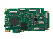 GX7_VenusEngine-1.png800 x 600 - 457K
 -
LOL.
Check topic title and contents. We are community who use and talk about all brands, not Panasonic reservation.
And I am confused about "new super sensor" and "performance features of the venus engine motherboard of the GX7".


Howdy, Stranger!
It looks like you're new here. If you want to get involved, click one of these buttons!
Categories
- Topics List24,082
- Blog5,725
- General and News1,396
- Hacks and Patches1,153
- ↳ Top Settings33
- ↳ Beginners256
- ↳ Archives402
- ↳ Hacks News and Development56
- Cameras2,393
- ↳ Panasonic995
- ↳ Canon118
- ↳ Sony156
- ↳ Nikon96
- ↳ Pentax and Samsung70
- ↳ Olympus and Fujifilm102
- ↳ Compacts and Camcorders300
- ↳ Smartphones for video97
- ↳ Pro Video Cameras191
- ↳ BlackMagic and other raw cameras141
- Skill1,960
- ↳ Business and distribution66
- ↳ Preparation, scripts and legal38
- ↳ Art149
- ↳ Import, Convert, Exporting291
- ↳ Editors191
- ↳ Effects and stunts115
- ↳ Color grading197
- ↳ Sound and Music280
- ↳ Lighting96
- ↳ Software and storage tips266
- Gear5,420
- ↳ Filters, Adapters, Matte boxes344
- ↳ Lenses1,582
- ↳ Follow focus and gears93
- ↳ Sound499
- ↳ Lighting gear314
- ↳ Camera movement230
- ↳ Gimbals and copters302
- ↳ Rigs and related stuff273
- ↳ Power solutions83
- ↳ Monitors and viewfinders340
- ↳ Tripods and fluid heads139
- ↳ Storage286
- ↳ Computers and studio gear560
- ↳ VR and 3D248
- Showcase1,859
- Marketplace2,834
- Offtopic1,342


