It allows to keep PV going, with more focus towards AI, but keeping be one of the few truly independent places.
-
Development and production costs of modern cameras are huge. And they will become much worse.
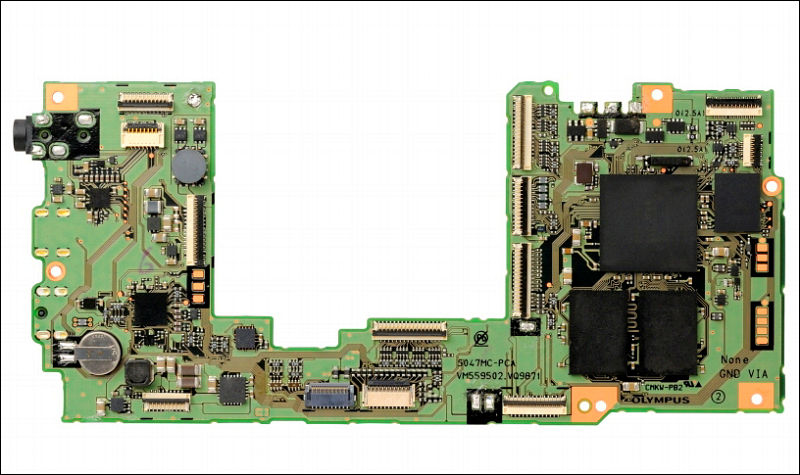
Check image of E-M1 main board above. Usually biggest chips in modern cameras are as follows : main LSI chip, one or more RAM chips, flash chips.
In some cases, like in some modern Panasonic cameras it can be something that looks like one chip only - with main LSI located directly below custom chip that contains both flash and RAM.
Development of all of the chips mentioned is very complex and costly task. But they have one core difference - you can get modern mobile RAM (DDR2 or DDR3 usually) chips, same is true for flash. But if you are serious company you develop your own main LSI. Sometimes it is join efforts, for example Nikon use Fujitsu FR image LSI as core for further modifications. Join development allow to save costs, but usually means that any problem of the partner prevents adding important features (like Fujitsu FR issues with video until last generation).
Another core difference between this chips is the process that is used to manufacture them. RAM and Flash usually are at forefront of progress, as they are simpler chips and development costs are lower with better yields and ability to compensate increased costs with instantly visible increased capacity.
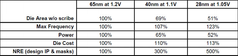
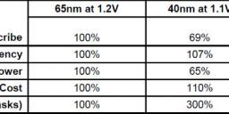
For LSI is much more difficult. Latest Fujitsu based LSI (like in Nikon) are still 65nm, as far as I know many other LSI are also in same or slightly smaller process. This is in the times were most mobile CPUs went 28nm. Why it is so?
Answer here is simple - development costs and ability to return investments. You can check table below:
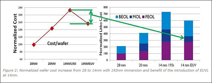
Further it become even worse:
Companies try to overcome this with existing process optimizations like SuVolta ones.
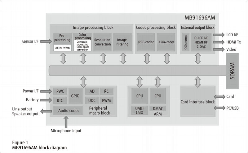
the MB86S22AA Milbeaut image processing chip — the DDC tech can cut power consumption by 30 percent, but it can still have twice the processing performance of comparable chips. Fujitsu and SuVolta have been working together since the Summer of 2011.
In case of new process costs rise even more due to problems associated with initial stages of production.
Charts from http://m.eet.com/media/1160433/sv_mw_b_120601_technology%20extension%20oped_revm.pdf
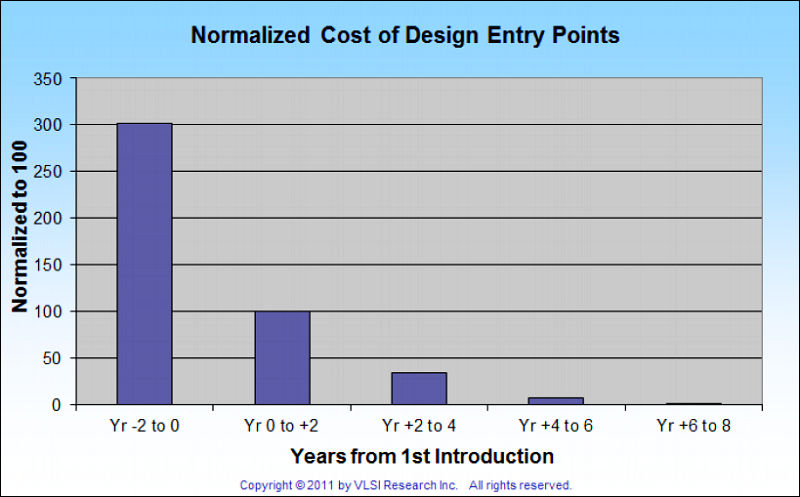
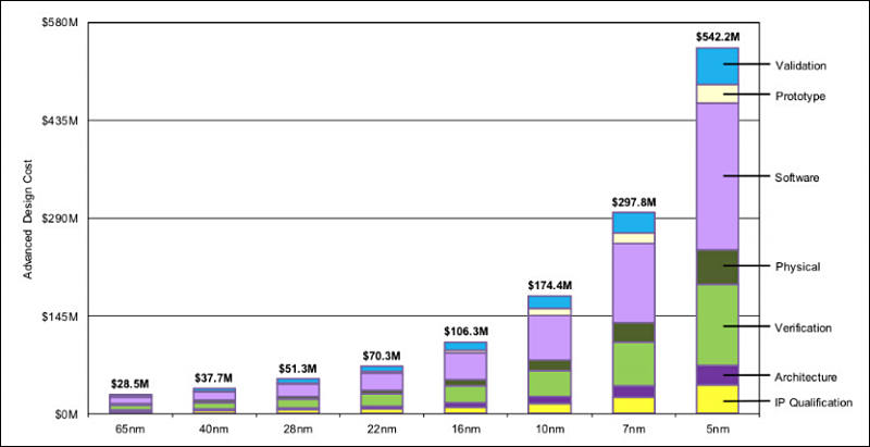
How big are this costs?
Non-recurring engineering costs estimates for 28nm complex image LSI are about $29 millions of dollars.In case of more iterations of development, producing more masks and modifications costs can be as high as $50 millions.
All this money must be returned from chip sales inside cameras. Millions of cameras.
Small companies usually have no chance to do it, so they use other solution - modern FPGA chips. We'll discuss in detail their specifics and development costs in next post.
So, as you see sharply declining sales of compact cameras do not start smile happily looking at your smartphone. Most of this cameras use same LSI as in big cameras, sometimes clocked down and with smaller amount of slower memory, but same chips. As otherwise it becomes impossible to be profitable.
Today all camera companies face complex problems:
- Necessity to move to 28nm (who did not do it already) and later to 14nm.
- Sharply rising development costs
- Declining overall cameras sales resulting in constant cuts and optimizations that have almost no effect.
- Steady or declining average camera prices (all companies went with idea to introduce premium cameras and design to rise the price)
In upcoming posts we'll touch FPGA development problems, 14nm costs comparisons, flash and ram issues, screens problems
 BM3.jpg800 x 189 - 43K
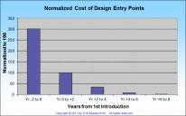 BM.jpg800 x 497 - 62K
 BM1.jpg800 x 510 - 59K
 BM2.jpg690 x 443 - 47K
 BM4.jpg705 x 275 - 43K
 -
this thread still going strong. And BM still using FPGA
-
It'll die slowly and painfully, so I reserved numbers :-)
-
Five years of this topic and we are still on part one? When, exactly will BMD die?
-
Cost of advanced mobile LSI with multiple CPU cores, quite similar to camera chips.
Note that all this years BM failed to move from FPGAs.
-
Doesnt matter
-
Fpga will never die. But its not energy efficient
You replied to your own though :-) As no one here said this.
-
Fpga will never die. But its not energy efficient
-
“FPGA is what you use when the volume is not large, FPGA is what you use when you’re not certain about the functionality you want to put into something,” he said on the call with analysts. “You can build an ASIC, a custom chip, that obviously can deliver more performance–not 20% more performance, but 10 times better performance and better energy efficiency.”
Head of NVidia.
P.S. FPGA are the core of both BM and Red cameras.
-
New 14mm fab delay
Intel Corp., the world’s largest chipmaker, said it will delay opening a new factory in Arizona.
“The completed Chandler plant, called Fab 42, hasn’t been filled with chipmaking gear,” Chuck Mulloy, a spokesman for Intel, said on Tuesday in a telephone interview. “The Santa Clara, California-based company decided to first upgrade the three other factories on the site because they can use existing equipment,” he said.
-
I'm not sure what is up with the doom and gloom in this thread.
This topic is not about doom and gloom as you like to say. It is topic about facts.
I'll be posting much more reasons soon as I'll have slightly more time, stay tuned :-)
-
Don't see a problem for BMD for quite some time. They already have well working cameras from image quality standpoint. In future versions they can focus on ergonomics, software enhancements, build quality etc. On processing side they can likely also partner with pana/oly or others if need be. I'm not sure what is up with the doom and gloom in this thread.
-
Intel's SoFIA SoCs designed for entry-level smartphones and tablets will be built using TSMC's 28nm HKMG process technology, said the sources. As for the other series of Atom SoCs codenamed Broxton, Intel will use its 14nm FinFET process to make the chips targeting high-end mobile devices.
Surprise, surprise. 14nm is first process were price is significantly higher and performance increase is very small.
-
So basically once you've gone with one image LSI brand you'll stick to it? And BMD is too small to enter such an agreement?
If I read their announcement correctly they are merging their LSI business (including image LSI?) into one new company... but if they will merge their product lines they didn't mention. And it may be too hard/give Panasonics competitors an advantage they may not want...?
-
couldn't BMD do the same? Perhaps with additional chips for any encoding duties, if necessary. Or is that not possible with the Milbeaut? Same goes to other brands, could, say Pentax or Nikon use an LSI for image acquisition and debayering, and a run off the mill ARM CPU for the interface and encoding duties? Something from say MediaTek or Realtek. They have got a ton of horse power. Heat could be an issue, but if the CPUs aren't stressed to much...
I hope you are not serious. Using of modern image LSI is possible mostly only via special agreement. Their usage also require vast knowledge and huge investments. In fact, it is why firms so hold to the same image LSI range.
Btw, no one told that Panasonic will use Fujitsu chips, they just made some join effort, we do not know that kind of stuff they are doing exactly.
-
I'm curious. Since Nikon is using the Fujitsu Milbeaut line as basis for their processors, and so does Pentax (not sure if they even modify the chips...), and soon it seems Panasonic (why...? Doesn't Panasonic have wonderful processors? The Milbeaut seems to be a bit lacking, at least in terms of video functionality)... couldn't BMD do the same? Perhaps with additional chips for any encoding duties, if necessary. Or is that not possible with the Milbeaut? Same goes to other brands, could, say Pentax or Nikon use an LSI for image acquisition and debayering, and a run off the mill ARM CPU for the interface and encoding duties? Something from say MediaTek or Realtek. They have got a ton of horse power. Heat could be an issue, but if the CPUs aren't stressed to much...
Also, what about competitors? Ambarella seems to have nice specs, though they are mostly used in smaller, cheaper cameras, and the GoPros.
Finally I wonder if the latest Milbeaut as used by Nikon and Pentax could do Cinema DNG, at least for 1080p? Where are the limitations? Is it just a matter of software + being able to write to the memory card fast enough? Or are the chips themselves limited... The Sony Bionz X seems to be very impressive. I wonder if Sony is working with another company, or if it is their own development.
-
Moore's Law is really more of an economic imperative.
-
moors law is bullshit
-
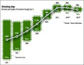
How many transistors you can buy for dollar:
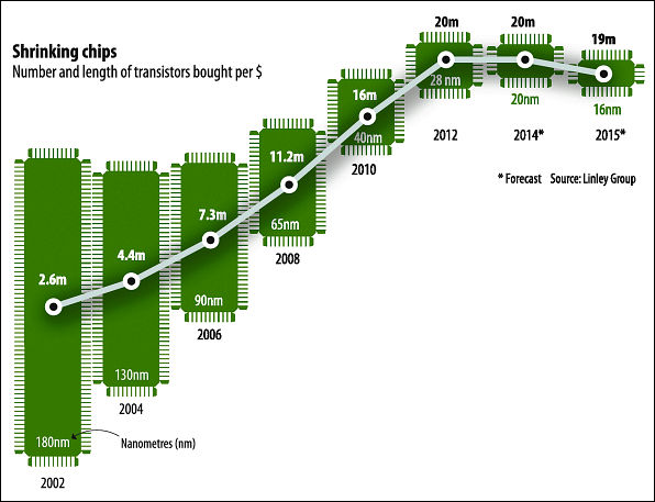
Good illustration of the things described here.
Thanks @agoltz for the link.
Via:http://www.economist.com/news/21589080-golden-rule-microchips-appears-be-coming-end-no-moore
 xa13.jpg596 x 457 - 52K
 -
How modern LSI looks from logical POV :
Check PDF in attachment also.
 olym5.jpg800 x 494 - 53K
 paper02.pdf1M
 -
@endotoxic They also have a lot of experience in the acquisition side of things; the Hyperdeck line seems to have been a significant source of investment for BM over time. We'll have to agree to disagree on the evolution of the lower-power general purpose CPU and its viability for image processing in the next few years.
@tomson8877 I don't think I've talked ill of any brand?
@DrDave To elaborate on what VK said, 3D printers tend to be pretty slow still. Also, if consumer printers are any indication, they require frequent maintenance and troubleshooting. For at least the next few years, they'll continue to be relegated to R&D divisions. I've heard some companies are working on 3D printers capable of creating semiconductors (which is pretty neat!), but I can't imagine using it at scale.
-
It is possible that technology will allow for inexpensive chip fabs, like from a 3D printer.
Problem is even for simple production 3D printers are mostly unusable. I am not even talking about "making chips". Right now each new step is significantly more expensive. Most companies are going fabless now with production concentrated in few hands only.
-
It is possible that technology will allow for inexpensive chip fabs, like from a 3D printer. The development is certainly a hurdle.
-
LOL.
Check topic title and contents. We are community who use and talk about all brands, not Panasonic reservation.
And I am confused about "new super sensor" and "performance features of the venus engine motherboard of the GX7".
-
@bannedindv @endotoxic @eatstoomuchjam @Vitaliy_Kiselev
Hi there, i´m not a techie at all, but i don´t get it why so much time is spent to talk some other brands ill? It would be nice if you could explain the possibilities of the GX7 or at least mention what panasonic delivered us.
We know the specification of the sensor which is obviously then new super sensor MN34320PL MAICOVICON.
There are pictures in the net of the hardware, can someone tell me please the performance features of the venus engine motherboard of the GX7.
 GX7_Sensor-1.png800 x 600 - 336K
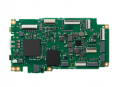 GX7_VenusEngine-1.png800 x 600 - 457K


Howdy, Stranger!
It looks like you're new here. If you want to get involved, click one of these buttons!
Categories
- Topics List23,980
- Blog5,725
- General and News1,352
- Hacks and Patches1,152
- ↳ Top Settings33
- ↳ Beginners255
- ↳ Archives402
- ↳ Hacks News and Development56
- Cameras2,362
- ↳ Panasonic992
- ↳ Canon118
- ↳ Sony156
- ↳ Nikon96
- ↳ Pentax and Samsung70
- ↳ Olympus and Fujifilm100
- ↳ Compacts and Camcorders300
- ↳ Smartphones for video97
- ↳ Pro Video Cameras191
- ↳ BlackMagic and other raw cameras115
- Skill1,960
- ↳ Business and distribution66
- ↳ Preparation, scripts and legal38
- ↳ Art149
- ↳ Import, Convert, Exporting291
- ↳ Editors191
- ↳ Effects and stunts115
- ↳ Color grading197
- ↳ Sound and Music280
- ↳ Lighting96
- ↳ Software and storage tips266
- Gear5,417
- ↳ Filters, Adapters, Matte boxes344
- ↳ Lenses1,580
- ↳ Follow focus and gears93
- ↳ Sound498
- ↳ Lighting gear314
- ↳ Camera movement230
- ↳ Gimbals and copters302
- ↳ Rigs and related stuff273
- ↳ Power solutions83
- ↳ Monitors and viewfinders340
- ↳ Tripods and fluid heads139
- ↳ Storage286
- ↳ Computers and studio gear560
- ↳ VR and 3D248
- Showcase1,859
- Marketplace2,834
- Offtopic1,319


