
It allows to keep PV going, with more focus towards AI, but keeping be one of the few truly independent places.
-
From sinhardware, copied from WBMachine
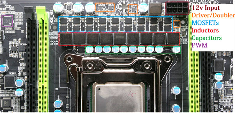
To begin talking about voltage regulators, and since this article is aimed at those without strong engineering backgrounds, we first will need to define certain terms which pertain to this article. The terms and definitions explain every part of the VRM and really will help, so please glance over them, because you will be wondering what the difference between the high-side and low-side MOSFETs are, and you need to read the definition of each term for things to make sense. You are basically getting a crash course in power supply design at a level that anyone who is interested can understand. So before the definitions I will give a quick analogy of how a motherboard VRM works.
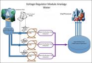
The water faucet analogy is slightly imperfect, however valid in many ways. Think about the process it takes for getting water out of your facet; the water has to be clean, at a decent pressure, and it needs to come in any amount you need it to. The power will be the water in this analogy. To produce the water in your faucet, water has to be controlled from a large source, cleaned, and then put into pipes and pressurized to reach your home. A CPU needs power like we need water, and the source for us might be a large lake, but from the CPU the source is your computer’s main AC/DC PSU(power supply). The water for us is then routed to a water treatment center, and that is basically what a VRM does. The water then needs to be pressurized and cleaned, that is basically what the phases do. The MOSFETs act like pumps, and the drivers are their controlling the pumps (MOSFETs) like valves (drivers). The inductors then store and clean the water like a purification tank, then all the purification tanks (inductors) send their water straight to the holding tank(capacitors) or straight to the city to people’s faucets. The PWM is the main control and the drivers (valves) are controlled by the PWM.

VRM: Voltage regulator module, this term refers to anything from a linear regulator to a synchronous multiphase buck converter, which is a switch mode power supply, which is what your motherboard's CPU VRM is. People also call the VRM the PWM, which isn't correct, PWM refers to a modulation scheme or a chip, not the entire circuit, however since PWM has a catchy ring to it people still refer to the VRM as the PWM. Some others may also call the VRM a VR or a VRC(voltage regulator circuit).
PWM: Pulse Width Modulation or Modulator, this is a scheme where phases are turned on and off in a pulse like manner, it can also refer to the control chip of the VRM. The PWM control chip does everything from turn on phases to monitoring different characteristics of the VRM, the PWM is the only part of a VRM that could be considered digital in nature, however it is possible to design the PWM with analog mechanisms(which is quite easy and popular).
Duty Cycle: The duty cycle is a ratio of Vout divided by Vin, so if there is a 12v input and a 1.2v output then the duty cycle is 0.1 or 10%, the duty cycle determines how long the high-side MOSFET needs to be on, and in this case it is 10% of the time to get 1.2v output. The duty cycle determines how often the high-side switches while the switching frequency determines how often it switches.
Switching frequency: This is the frequency at which the VRM switches or pulses. Increased switching frequency means that the current will move more quickly throughout the VRM, however while increased switching frequency helps with transient response and helps to decrease ripple, it also reduces efficiency and increases temperature. With a low duty cycle the switching frequency is also limited. The switching frequency determines how often the phases switch or pulse. So if the switching frequency is 300khz then the phases pulse 300,000 times per second or pulses once every 3.33 microseconds(usec) or 3.33e-6 seconds. Switching frequency also needs to be constant along phases, so if you double the phase count you should also cut the frequency in half for each of the doubled phases, if you don't do this, then the entire effective switching frequency of the entire VRM can double and lead to issues unless already accounted for.
MOSFET: Metal Oxide Semiconductor Field Effect Transistor, basically a simple switch which can turn on (connect the source and drain) if a voltage is supplied to the gate. There are usually 3 points to a MOSFET, the gate which is used to control the MOSFET, the drain which is where the current flows to, and the source which is connected to the source of the current. A MOSFET is basically a switch/electronic valve. This is easy to think about, when a certain voltage is supplied to the gate, the source and drain are then connected for current to flow freely. By the way FET is MOSFET for short.
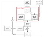
High-Side MOSFET: This MOSFET has its source connected to an input, usually 12v in modern VRMs, and its drain is connected to the inductor / source of the low-side MOSFET. The driver controls its gate. The high-side MOSFET's switching losses are very high as it will be pulsed very quickly. When a phase is ON, then the high-side MOSFET is also on. The duty cycle determines how long the high-side MOSFET stays on. The high-side MOSFET limits the current output of the phase. High-side MOSFET is also called the Control MOSFET.
Low-Side MOSFET: This MOSFET has its source at the inductor / the high-side's drain, the low-side's drain is connected to the ground. This MOSFET is in charge of turning on when the phase is off, and it completes the circuit and allows the inductor to discharge all of its current. The conduction losses of the low-side MOSFET are very important as this MOSFET will stay on longer than the high-side. The low-side MOSFET is also sometimes called the synchronous (or sync) MOSFET.
Inductor: Also known as choke, this is an energy storage/filter component. It is made up of a thick coiled wire either surrounding and/or surrounded by some metal casing. This is probably the most recognizable part of a VRM, as it is the metal cube each phase has. The inductor stores energy in a magnetic field. The inductor is the ultimate limiter of the output current of each phase, the saturation current is the maximum current that the inductor can sustain.
Capacitor: Most people know what a capacitor is; it is a sheet of thin metal put up right next to another sheet with a di-electric in between, then the sheets are wound into a circle and they are cased in metal. The capacitor stores energy in an electric field opposed to the magnetic field the inductor uses. Electric and magnetic fields are related by the way.
Driver: In a VRM a driver isn't the dude who drives you around in a limo, but instead it is a chip which controls the MOSFETs in each phase. The driver is controlled by the PWM and is an integral part of the system.
Doubler: We will talk about the doubler a little as they are commonly used today in the phase wars. They basically are like a multiplexer which takes a single PWM signal and divides that signal into two, however it also reduces the maximum switching frequency by half. There are also some quadrouplers, these are interesting as I have only seen one which is in production(IR3599) and it takes a single input and basically divides it into 4 by dividing into 2 twice, and you get an output which is ¼ the switching frequency of the input. Nowadays we see single doubler chips, or we see them integrated into the driver, however in the past sometimes motherboard makers used analog switches, which would take in 4 PWM signals and output 8. The only place you see this done now is with some X58/Z77/Z68 MSI motherboards.
 sa6642.jpg800 x 385 - 91K
 sa6643.jpg800 x 552 - 63K
 -
The PWM Controller: the story of the multiphase buck converter.
The first part of the VRM is the PWM control chip; each PWM has a certain number of PWM outputs, anywhere from 1-10 PWM outputs. The PWM works with a negative feedback loop, this loop monitors voltages, current, and temperature and then uses the user defined voltage requests to change the PWM outputs to move towards what the user requests. Each PWM output carries the switching frequency and the duty cycle. The duty cycle controls the voltage output, as it controls how long to turn on the high-side MOSFET. The switching frequency is the rate at which the phases should switch and is measured in the KHz range, anywhere from 100khz to 2000khz. So if the switching frequency is 300,000hz or 300KHz then the phases pulse once every 3.33 microseconds. If the duty cycle is 10% or 0.1 then 10% of the time the high-side MOSFET needs to be on and the low-side will be engaged the remaining ~90% of the time. There is also dead time between switches so more like 85% of the time the low-side MOSFET is engaged.
Below are samples of PWMs:
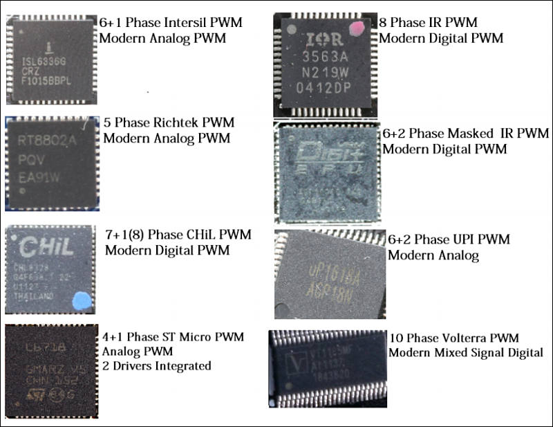
The difference between the analog and PWM control method rests in how the PWM controls its feedback loop. In analog PWMs the feedback loop is an analog signal, but in digital PWMs they use an analog to digital controller to convert the inputs into 1s and 0s for a mini processor to analyze and control. Digital PWMs also contain on-board memory and are really the wave of the future. Analog PWMs have traditionally been a bit faster, however advancements in ADC technology has made digital control loops quicker.
Drivers and Doubling Schemes:
PWM and Driver relation: The PWM signal is sent to a driver, the driver then is able to take the PWM signal and control the MOSFETs in the phase by turning on or off the gates of the MOSFETs. If a doubling scheme is used then it usually occurs before the PWM signal hits the driver, usually a chip is used to increase the number of phases and divide the effective switching frequency in half.
PWM signal versus Driver Signal: So the PWM signal goes from the PWM chip to the driver, and the driver outputs driver signals to the MOSFETs. So why do we have both? The reason being that the PWM signals can be safely translated across the motherboard, for instance the switching frequency is decoded by the driver easily as the PWM signal is pulsed at the switching frequency. The driver signal on the other hand needs to be at a certain voltage to turn on and off the MOSFET's gate, and if it isn't exactly at a certain voltage the MOSFET might not turn on, thus the drop in voltage over a distance can affect the usefulness of the driver.
Below are a bunch of different driver and doublers, and the reason we are covering both in one page is because many times they are integrated into a single chip.
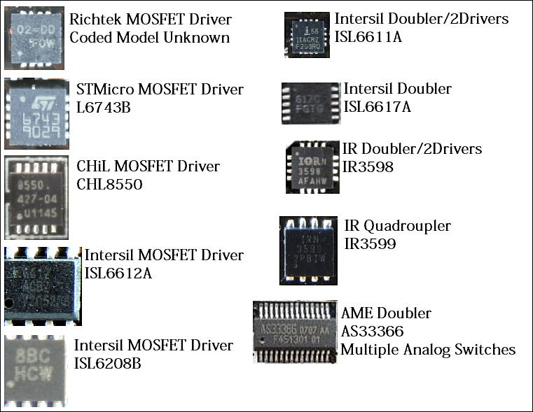
A doubler is a simple circuit, it just takes in a PWM signal and cuts it in half, earlier doublers were analog switches, in which they would split a bunch of signals on one side and then combine a bunch of signals on another. Doublers have to be able to take in current monitoring signals and combine them for that phase, as the PWM requires this current readout for operation, so it is a two way exchange.
Methods of PWM driver and doubling schemes
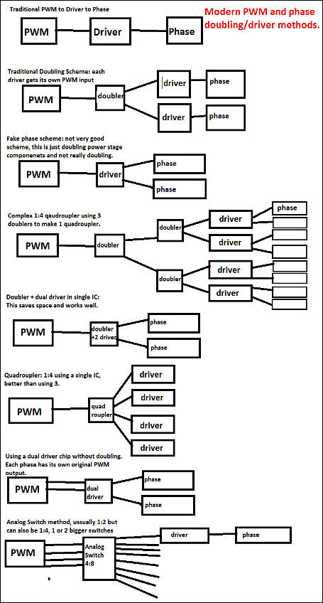
Now there are many doubling schemes, however in my opinion a phase is only a phase if it has 3 things; a driver, a high-side MOSFET, and a low-side MOSFET. The inductor is granted, however the issue is when some manufacturers think they can get away with doubling the number of MOSFETs and inductors without increasing the driver count. This is a very cheap and not very good way to double the phases. Just adding components means that you will have double the switching components with the same current output because the current of both those phases needs to be added up as a single phase. You also aren’t cutting the switching frequency in half like you should, because the phases add up together. So you must use a doubler to double the phases.
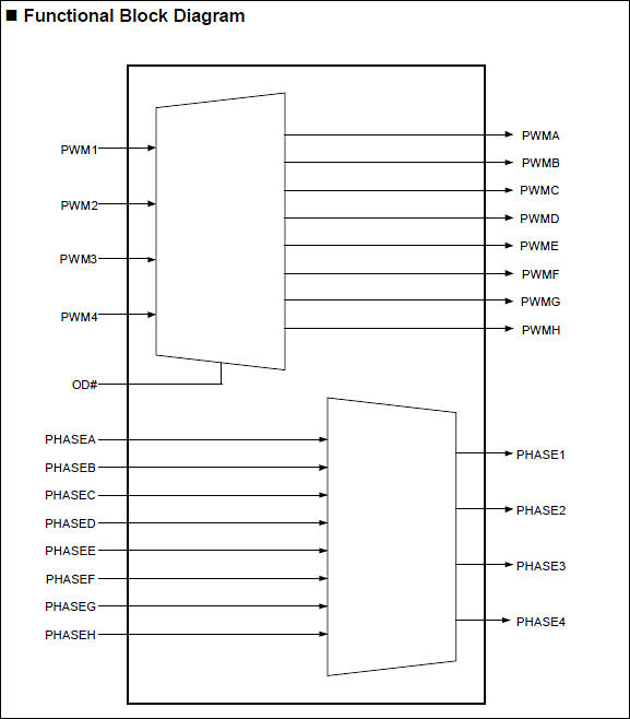
This is a basic analog switch doubling method. As you can see the PWM1-4 are inputs from the PWM, and the Phase1-4 are the current monitoring inputs to the PWM. You can see that the PWM signals are split into two while the current monitoring is combined on the way back. For a doubler to work you must be able to provide the current monitoring back to the PWM. You don’t need anything for temperature or voltage monitoring because they are measured at the end of the loop (voltage) and independent of each phase (temperature).
Later one we will go over some of these extreme doubling methods with examples of extremely high-end 20, 24, and 32 phase VRMs all using different doubling methods.
 sa6644.jpg800 x 617 - 72K
 sa6645.jpg761 x 589 - 73K
 sa6646.jpg455 x 848 - 82K
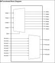
 sa6647.jpg577 x 658 - 43K
 -
The MOSFETs:
MOSFETs are extremely interesting things, they are the root of all electronics as they are a basic example of a transistor. There are many types, and those found on modern day VRMs are all N-Channel. In the past a phase was only made up of a high-side MOSFET and a Diode (instead of a low-side MOSFET) this is called an asynchronous buck power stage. The high-side MOSFET would provide the power and then after a diode would engage to complete the circuit, however losses from the diode weren't very small. Someone figured out that replacing the diode with a low-side MOSFET would reduce power loss and increase efficiency. Thus the synchronous buck power stage was born and has been used on motherboards ever since.
So why do you need the low-side MOSFET or diode? The answer is that when the high-side MOSFET cuts off its power the flow of current through the inductor stops, and with nowhere for the current to go the inductor will go a bit nuts and might result in a huge voltage spike. So the diode or low-side MOSFET will need to engage not only to prevent this, but also to allow the current to continue flowing in the same direction.
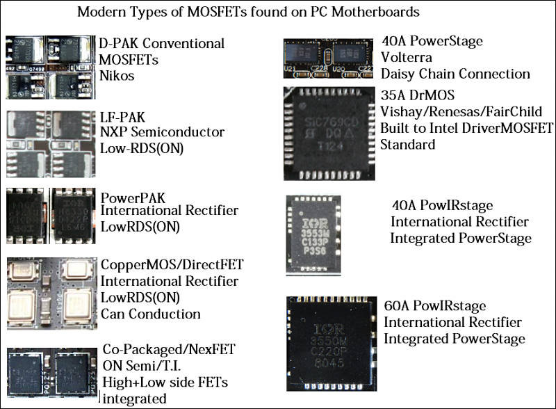
Because the high-side MOSFET provides all the power, it is the first limit point within the power stage. However rating MOSFETs power output is VERY difficult as there is no standard for comparing them. One has to keep in mind two things while viewing MOSFET ratings; temperature and power loss. MOSFETs usually can output current better at lower temperatures, however they also come with high power losses as well. For instance the 60A IR3550 is rated at 60A at 25C and 11W, however if we look at a typical NXP PH7030AL which is found on many motherboards from ASUS and ASRock, it is rated 68A but at 62.5W and 25C, so basically it gets as hot as a CPU just to output 68A, compared to the IR3550 you could use 5-6 IR3550 and output 300-360A at the same power loss as a single PH7030AL from NXP. However the IR3550 is the king of the hill when it comes to MOSFETs, and it is a totally integrated power stage which means it will inherently have higher efficiency.
One very interesting MOSFET is the DirectFET from IR, the technology from the DirectFET is used in the IR3550. One way that the high-side and low-side are connected in both is by body conduction. That means that the current will flow through the entire body of the MOSFETs instead of through a connecting trace or plane. That is one reason that the DirectFET have a metal body, because the current flows through it instead of inside.
MOSFET size is also interesting to note, the IR3553 listed above is a 40A part and is almost ½ the size of the IR3550 which is 60A, however the DrMOS listed above is a 35A part and is as large or larger than the IR3550. That just goes to show you how much integrated power stage technology differs from product to product. Also 11W power loss is pretty big let alone 62.5W. MOSFETs have many interesting characteristics, you can actually think of them as a resistor and capacitor. So when size comes into play the capacitance is greatly affected while resistance is also affected but not as much. What is important is the technology and material that goes into the MOSFET.
Dead Time: There are times when neither MOSFET is on, and this is called dead time. A Schottky diode will reduce losses from that dead time if used. Also, the driver is in charge of the dead time and the time each MOSFET is on. It has to watch and exactly switch the MOSFETs at the correct time to avoid any voltage shoot through.
 sa6664.jpg800 x 588 - 92K
 -
The Inductor and Capacitor: Together they are the output filter.
Output filter design is very important, together the inductors and capacitors must work in unisons to provide constant power to the CPU. This might not seem like a big deal, but in a split second the CPU will go from 0.9v at 10A to 1.35v at 130A, or even 1.5v at 200A and the VRM must be able to supply the correct current and voltage without any delay. This is especially hard because the CPU will also step down and back up many times per second with the above requirements. When you start some computation then the CPU needs power to complete it, and the VRM is the provider of that power.

The inductor: Also known as a choke, inductors come in many varieties. Some are metal alloy, while others are ferrite; they have different numbers of turns of a copper coil and can store energy in a magnetic field. They are also rated at a certain inductance. Higher inductance means that the inductor will store more energy but also be much slower to discharge. The inductor is a very interesting magnetic component, it stores energy in a magnetic field and it also acts as a filter, it doesn't change up the DC voltage running through it, however it will filter out most of the AC voltage. The inductor also has one other major property which is beneficial for VRMs, that is that it opposes changes in current. The inductor isn't a fast component, meaning that it can't instantaneously discharge all the current, this happens over a longer period of time after an input current has stopped. What we have to realize is that the input to an inductor is pulsed at the switching frequency in most cases, and the output of an inductor gets rid of those pulses. You can measure the switching frequency at the leg of the inductor which is hooked up to the MOSFETs, but at the other leg of the inductor you will only measure 60hz (the fundamental frequency in the US). You can easily see the pulses of current from the high-side FET have been equalized, what is more interesting is that the inductor will tend to average the current from the pulses, and that is very important.
Inductor's max current: Inductor's have something called Isat which is their saturation current. This should be the maximum current applied, however sometimes the VR will need more power and more current will be introduced. If this happens then magnetic flux will flood the core of the inductor, and then the current will skyrocket and that can blow up the MOSFET. You can see this happen with the GTX570's VRM, there they use those small low current inductors from laptops, and then when users go to overclock they blow a MOSFET. Also inductors get hot because of power loss, just something to remember, just because they are hot doesn't mean they will blow.
Coupled Inductors: Coupled inductors are very interesting and complex (expensive) inductors, they basically are two coils which don't touch in the same shell. Only a few VRMs use coupled inductors, and they aren't common because of the sophistication of the design of the parts required, mainly that of the inductor itself. However if you want to see what a coupled inductor looks like, take a look at most Volterra based VRMs, like the one of the X58 Classified. Later on we will cover famous VRMs.
Capacitors: Now capacitors come in many different shapes and sizes, and they store energy in an electric field and they charge and discharge faster than inductors. They are usually also more expensive, and you need a bunch of them in different types for every VRM. Capacitors act as energy storage and they are crucial to making the VRM work. They do clean up the output a little, and they are used to power the CPU when no one else can. Usually two types of capacitors are used, those which aren't good with high-frequency and higher frequency. Lower frequency capacitors are those you usually see, the can-type capacitors, but the high-frequency capacitors are the little ceramic MLCC. ESR (equivalent series resistance) and inductor ripple current determine output ripple. However ESR is also inversely affected by bulk output capacitance. So if you increase the bulk output capacitance you also can lower the output ripple.
The low Pass Filter: Together the caps and the inductor form a low pass filter or an LC circuit (L= Inductor, C= capacitor). Since they are the last part of the output they can limit the transient response. Higher inductance limits transient response, however multiphase design allows each phase to operate on its own, and thus you can use less inductance per phase with more phases(compared to just a single phase). This is important because the inductors aren't fast enough to keep up with the transient response demands, thus the capacitors come into play. During an initial transient let's say from 10A to 150A the high-side MOSFET will stay on for a longer period of time, however the inductors won't quickly be able to output this higher current, thus the capacitors come into play and they will provide the current needed until the inductors can output the majority of the current. Then when the CPU goes back down to 10A the capacitors will charge up again with the extra energy. There are many ways to build the low-pass filter, and we will go over some of those ways later on.

 sa6648.jpg881 x 656 - 113K
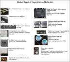
 sa6665.jpg800 x 709 - 83K
 -
Let’s Put it all Together!:
Now you should know exactly what each component does and how they work together, however there are some more things we should go over.
This is a single phase VRM in a block diagram:
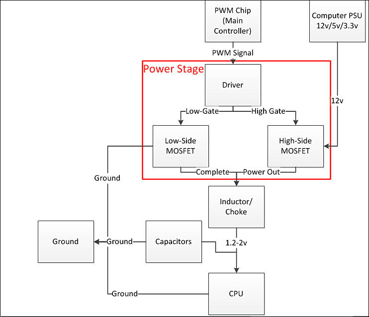
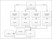
We can add these up to a multi-phase VRM:

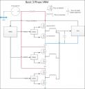
Now it is important to see it as an electrical diagram:
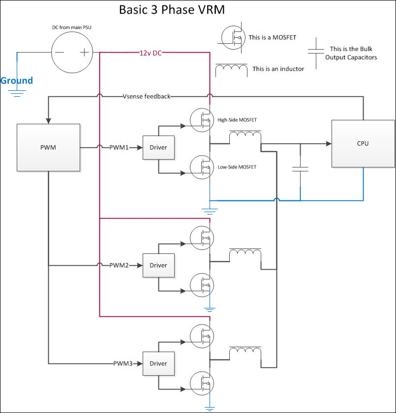
During operation PWM 1 will pulse at the driver and the driver will turn on the high-side after turning off the low-side MOSFET in phase 1. Then the current will charge up the inductor. Then PWM2 will pulse driver 2, and then PWM 1 will turn off the high-side of phase 1 and PWM2 will turn on the high-side of phase 2. When PWM3 is pulsed then the other phases will also have their high-side off. However it is possible for all phases to be pulsed at the same time if a lot of power is needed. It is okay for the high-side to be on for different MOSFETs. When these phases reach their needed output they are turned off, the amount of current each phase provides is monitored directly by the PWM during operation.
Why do we use multiple phases instead of one big one?
What is phase interleaving?The answer is not so complicated. We can look at this question from many ways, and we will do so now.
- First off is transient response of the inductor. If we have a single phase and very high current requirements then we will have to expand the energy storage of our components. However increasing the energy storage of the inductor also reduces the transient response of the system. So using many inductors with lower per phase inductance will allow for faster transient response.
- If you have a single phase the chances are that there is going to be a lot of heat there, so spreading the phases across a larger area and increasing their count can help reduce heat and increase efficiency. However it is important to note that switching losses do become greater with more parts. One must also think about the amount of current the copper in the PCB can transfer over a small area of space, a single phase as big as a normal phases in a multiphase VR can’t output 300A, but spread that over 6 phases and 6x the space and it is only 50A per the same space.
- The interleaving effect is by far one of the most beneficial effects of having more than 1 phase. Because of how the phases operate out of phase with each other the total ripple frequency can be multiplied by the total number of phases. This huge increase in ripple frequency decreases ripple amplitude and ripple current. This helps reduce both input and output bulk capacitors requirements. If you skip down a little bit then you will see how more true phases can decrease current.
What does it mean when the phases are out of phase with each other?
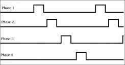
Each phase works out of phase with the other phases and that means that each phase is on when the others are off. Being on means your high-side MOSFET is ON, being off means your low-side is engaged.

This diagram shows that each phase is pulsed on when the others aren’t being pulsed on. This is what leads to interleaving. The interleaving effect also has its own limitations.
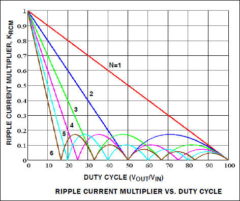
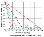
From the ISL6366 Datasheet we can see how they have measured the effectiveness of interleaving. N=the number of phases (channels from the PWM). You want to be as close to 0 ripple current as possible. However notice the duty cycle, the worst part of all this is that going from 12v to 1.2v is a 10% or a 10 duty cycle above. So having 6 phases would reduce the ripple almost 50% when compared to a single phase at 10% duty cycle. Moving to 8 phases would improve this a tiny bit, but not as much as going from 5 to 6 phases. However with the small duty cycle of modern day VRMs, every little bit can count.
Adding n a doubler
Now we can toss in a doubler to see how the doubler will affect the pulses and whatnot. For simplicity we will look at a very basic doubler, going from 1 phase to two phases:
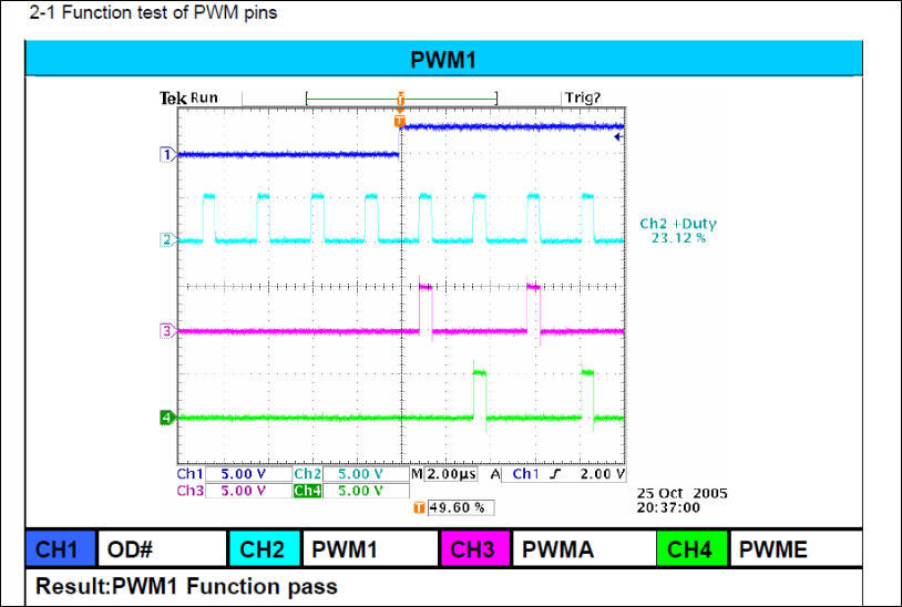
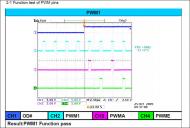
The light blue represents a single PWM channel/phase from the PWM pulsing. The pink and green then show us what the doubler does. The doubler will call one of its doubled phases every other time the main PWM line pulses. If you have a quadroupler, then only one of its four phases will turn on when it is pulsed, thus every four cycles of the main PWM, the quadroupler will have pulsed each one of its phases. This can lead to much better thermal distribution which will decrease the stress on each phase. However there is another operation mode in which all the phases are pulsed on, and in that operation mode the doubled phases have half the load on them as they would if there were half the number of physical phases. Sometimes it is required to pulse all phases beucase of a huge current step, then you need all the power you can get as fast as you can get it, and turning on the phases is the best way to do this. Otherwise in normal modes of operation it is useful to use only a single phase at a time.
Phase Shedding: Many times it is not needed to use all of your phases, and in that case the VRM will shed phases from the main PWM line, however shedding correctly with doublers requires a very well synced and powerful PWM doubling scheme.
We have covered most everything you need to know about the VRM basics, now let’s move to see some of the best VRMs ever designed and produced.
 sa6649.jpg742 x 638 - 50K
 sa6650.jpg776 x 587 - 40K
 sa6652.jpg805 x 841 - 59K
 sa6653.jpg715 x 373 - 26K
 sa6654.jpg472 x 396 - 53K
 sa6655.jpg814 x 548 - 71K
 -
Primers are from old boards as in original article
EVGA X58 Classified
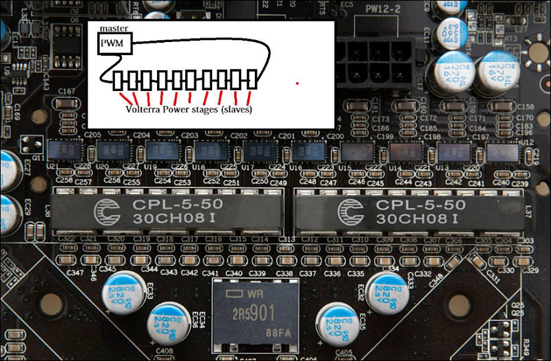
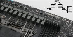
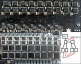
This VRM is extremely unique in its form and function. First of all you can notice it uses coupled inductors. These inductors are actually made custom for this VRM, and thus cost is extremely high. Another aspect that makes this VRM very unique is that it is the only true 10 phase PWM, the VT1185M. The power stages are VT1185SF which are rated at 45A per phase, in the past they have VT1195 which was 40A, the CPL inductors however only allow 40A per phase. There is a 900uF Proadlizer and then lot of MLCC, and only 4 normal polymer can-types are used. This VRM worked at 800KHz to 1.33MHz and thus is a very high frequency VR. Volterra’s PWM VT1185MF can switch up to 1.33mhz and this VRM does operate at much higher switching frequencies compared to normal VRMs, and it is known to get pretty hot. What is most interesting is how the phases are linked to the PWM, instead of each phase having its own PWM channel, the volterra system works on a master with slaves, and the slaves are linked to each other in a circle with the master PWM, look at the paint drawing on the picture for more details.
 sa6656.jpg800 x 524 - 111K
 -
ASUS Rampage 3 Extreme
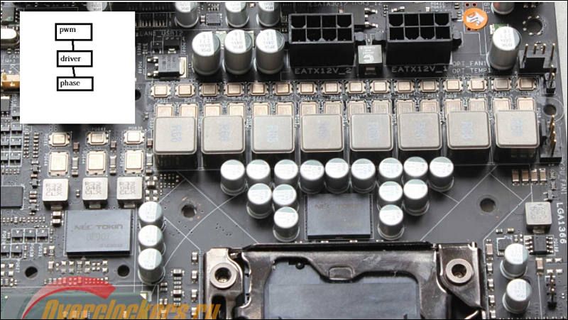
This VRM is highlighted because of its high tech use of components. We first have sets of DirectFETs, 4 per phase, and 8 phases true from the 8 phase CHL8328. The DirectFETs are interesting because current runs through them instead of the board. ASUS chose to use Trio Metal Alloy 0.68uH inductors which have a 35A saturation current, so each phase can do 35A. The output is made up of a lot of polymer can-type capacitors as well as a single NEC Proadlizer.
GIGABYTE X58A-OC
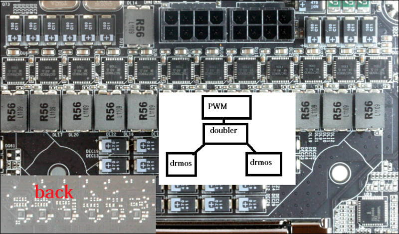
Next we have a more traditional VRM on the X58A-OC. It is only 6 phases true at the ISL6336 PWM and ISL6617 doublers are used to double the phase count. However what is pretty significant is that GIGABYTE chose to use some very high current 50A inductors for each phase. Along with 35A DrMOS from Vishay, and almost 9000uF of POSCaps.
GIGABYTE Z77X-UP5 TH
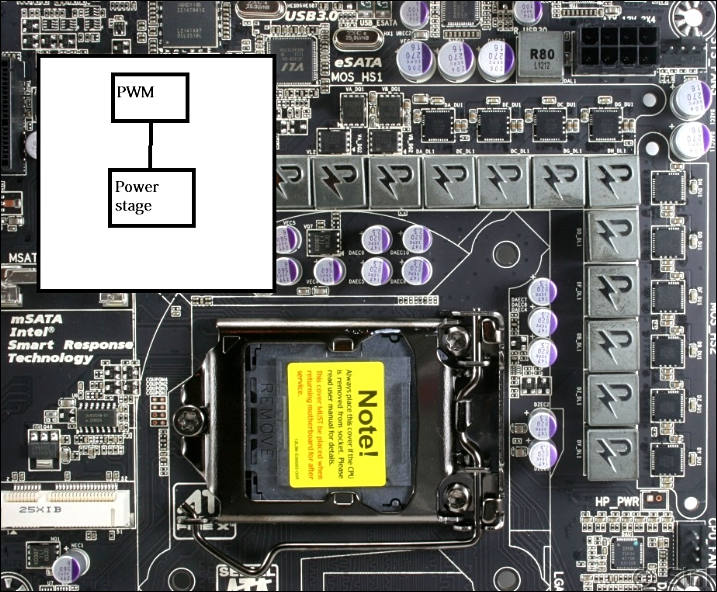
The Z77X-UP5 carries the highest power density in the market today. With the capability for a true 60A per phase, this VRM is loaded with power density. The most advanced parts is the IR3550 power stages, which are designed to produce 60A output in real circumstances. However alone they wouldn’t be much without the 60A inductors, custom made for this implementation. There is also a true 8 phase PWM the IR3563A, IR states their newest PWMs can do up to 2MHz per phase, the IR3567B has this 2mhz figure in its datasheet. This VRM has the highest output per phase.
 sa6657.jpg800 x 451 - 83K
 sa6658.jpg800 x 469 - 93K
 sa6659.jpg717 x 592 - 109K
 -
MSI X79 Big Bang X-Power II
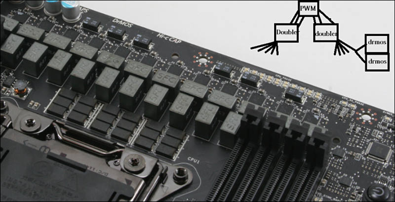
Now we can take a look at some monster VRMs. MSI tends to use the analog switch method for their phase doubling because of their vendor, uPI. However there isn’t enough doubling technology to support 20 phases independently, that means that the PWM can have 5 phases doubled to 10 phases, and then those 10 are routed to two DrMOS each to get a 20 phase VRM.
GIGABYTE’s Z68X-UD7
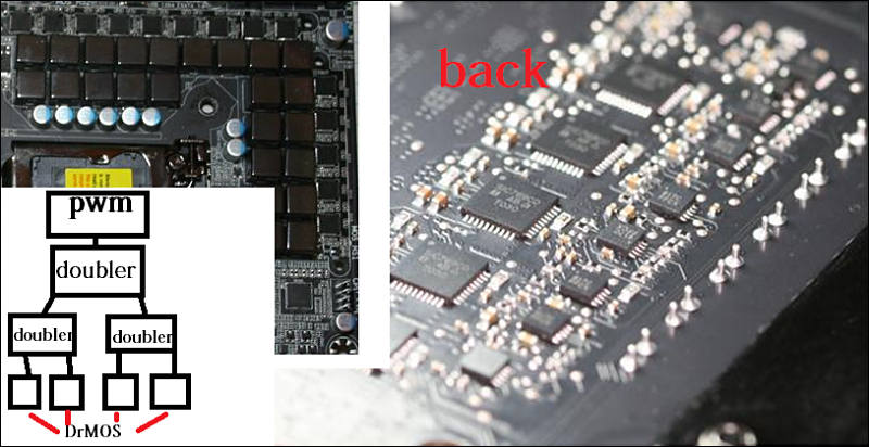
This was one of GIGABYTE’s 24 phase designs. The most interesting was that of the X58A-UD9 which used two 6 phase PWMs to get 12 phases and then they doubled those to 24 phases. However the P67A-UD7 and Z68X-UD7 use a much different method. They only use a single 6 phase PWM, and then they use 18 doublers, 6 for the first stage and 12 for the second which successfully quadruple the 6 phases to 24. Then 35A DrMOS are used.
GIGABYTE’s X79-UD7
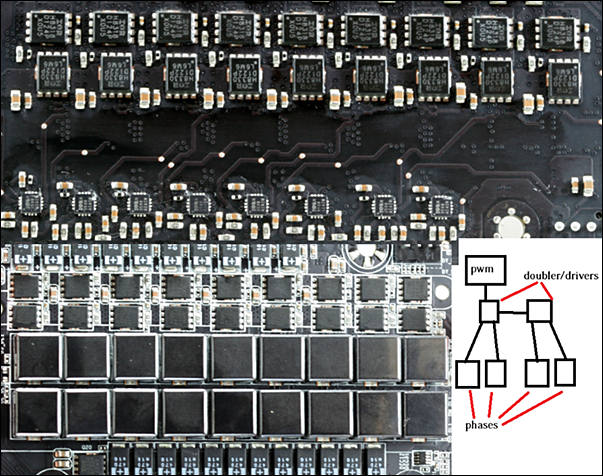
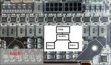
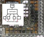
Here we have a very odd doubling scheme. This was GIGABYTE’s first round with a digital PWM from IR, and they used IR’s doubler/dual drive the IR3598 as well as their MOSFETs. They had a 16 phase VRM, however their PWM the IR3567 is only a 6 phase. So they used 4 phases and linked the doublers as in the paint diagram in the picture. This isn’t exactly the best way to double, however it is a valid way as the IR3598 have the ability for dual input and have this cascade mode built into them. This is a very unique doubling method which hasn’t been used since.
Here we have the last and highest output VRM the GIGABYTE’s Z77X-UP7
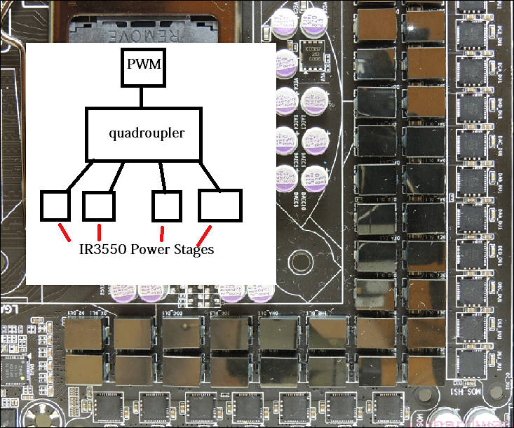
GIGABYTE’s went all out with their Z77 and X79 UP boards. They took Ultra Power to another level. Here we see the use of a 32 phase VRM, this 32 phase VRM is based off of a IR3563A which is 8 phases, then each of those phases is routed to a IR3599 a quadrupler, and then you get 32 phases total. What makes this more interesting is that they used 32x IR3550!! That is a huge cost and definitely added to the cost of the board. This is however the only UP board which doesn’t use the 60A inductors, and thus 60A per phase isn’t possible. However they did a live demo at 2000W output, each of these SMD mounted inductors is capable of 25-30A per phase, because to do 2kw at 2.4v you need at least 26A per phase. This is the most monster VRM ever put on a motherboard and sold to the people.
 sa6660.jpg800 x 409 - 57K
 sa6661.jpg800 x 412 - 65K
 sa6662.jpg603 x 476 - 83K
 sa6663.jpg733 x 610 - 110K
 -
Now PV specific part by me
As you remember you live in capitalism and it is marketing and companies PR that is driving things around, just physics and it's laws sometimes have to bent a little:-)
First, phases number, marketing thing number one
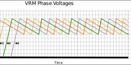
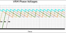
Visual illustration advantage of having more phases:
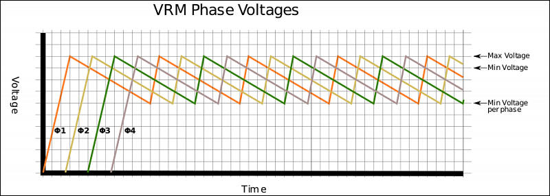
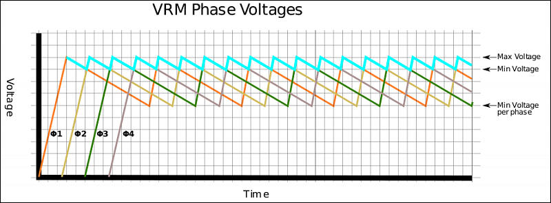
In reality it is all very smooth due to 300Khz-1000Khz switching frequency.
But believe me, processors are designed to normally work with worse case scenario. As 90-95% of motherboards will be cheap ones and lot even custom models made for corporations and cheapened further to allow manager to get bonuses from savings.
More is better, but in reality after 3-4 phases it is hard to grasp outside extreme overclocking (meaning rising voltage and running 8 core CPU with heatsink not producing good air flow around VRM area).
Also note that this same expensive motherboards have 2 phases for SoC IO and GPU parts of CPU and no one complains about voltage stability here. If this had been issue everyone had some talk around. RAM frequently can have even one phase design and no one complains also.Second, MOSFETS and phases again
Let's get cheap small B350M Bazooka, RT8894A PWM controller, 4 phases, PK616BA high side MOSFET and pair of PK632BA low-side MOSFETS.
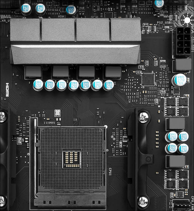
Why only one side is paired and other is not? Thing is that our PWM is transforming 12V into around 1.35v, so duty cycles for PWM will be around 11%. So, MOSFETs are open/closed for very different amount of time, and bulk of load lies on low-side MOSFETs. Each transistor being open has non zero resistance so it heats (RDS(on) in specifications) , and as one side is open almost 10x more it is smarter to double it . Doubling MOSFETs halves the current through each and doubled the heat transfer area effectively dropping each MOSFET temperature.
Lot of heat and losses actually happen during switching, so it is less heat being produced at 300Hkz compared to 1000Khz as it is more than 3 times less switching events.
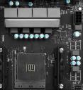
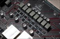
Now let's see MSI X470 Gaming Plus - same RT8894A PWM controller, 4 true phases with doubling of elements, pair of 4C029N high side MOSFETs and pair of 4C024N low-side MOSFETS. X370 model actually had exact same MOSFETs even as in Bazooka.
Looks like this without heatsink:
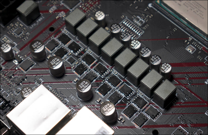
So, we now have one extra high side MOSFET and extra choke per phase (capacitors are same). Low side MOSFETs have around 18% less resistance. Both made mostly for marketing purposes and add not too much into real performance. Thing will be only little cooler, but only little.
 sa6667.jpg800 x 286 - 51K
 sa6668.jpg800 x 296 - 53K
 sa6672.jpg735 x 802 - 122K
 sa6670.jpg800 x 520 - 87K
 -
How it looks on oscilloscope
-
VRM cooling
On most motherboards now VRM coolers are awful and made by designers for looks instead of doing their function.
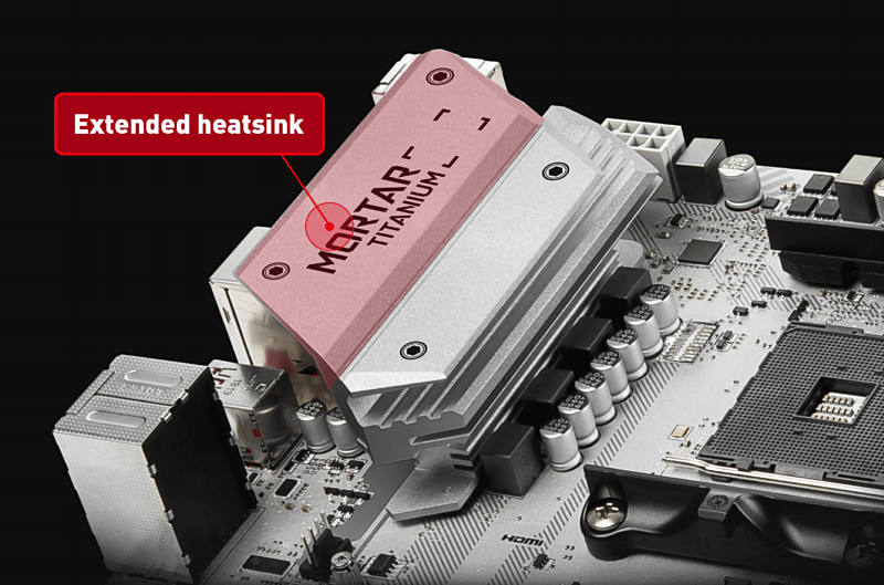
This is primer of bad one, but lot of much worse are around, just one brick of aluminum with nice looks.
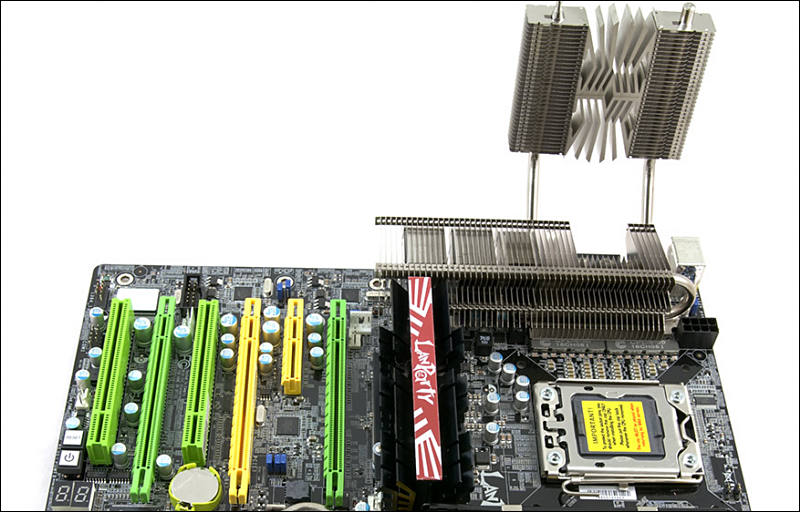
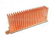
Good heatsinks must have big dissipation area, copper is better and heatpipe, if properly made, helps.
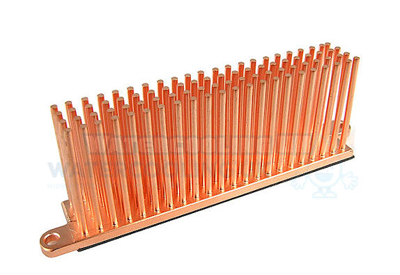
Such is around 10x more efficient in heat transfer.
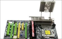
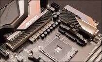
On top board you can see such heatsinks:
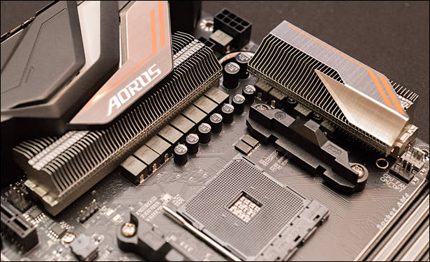
It is better, but designers put covers that degrade performance.
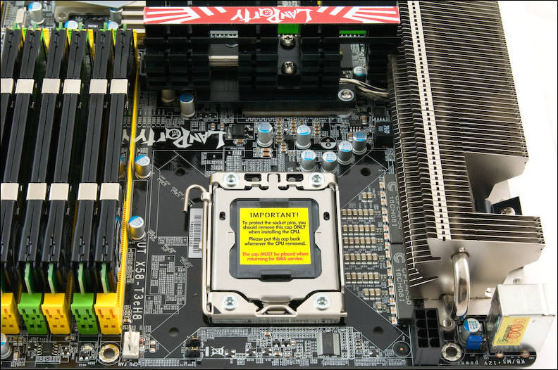
Primer of very good heatsink from older era (DFI LANParty UT X58-T3eH8 board), it uses help of 12cm exhaust fan.
 sa6844.jpg800 x 529 - 71K
 sa6845.jpg574 x 395 - 41K
 sa6848.jpg800 x 512 - 80K
 sa6849.jpg616 x 376 - 63K
 sa6851.jpg792 x 526 - 122K
 -
Modern motherboard VRM samples
Gigabyte Z370 AORUS Ultra Gaming

- ISL95866 PWM controller
- 4 phases for VCC:
- 2x 4C10N highside MOSFETs
- 2x 4C06N lowside MOSFETs
- 1 inductor per phase
- 3 phases for VCCGT:
- 1x 4C10N highside MOSFET
- 1x 4C06N lowside MOSFET
- 1 inductor per phase
Three drivers already present in PWM controller, only 4 extra are used.
ASUS ROG Strix H370/B360-F Gaming
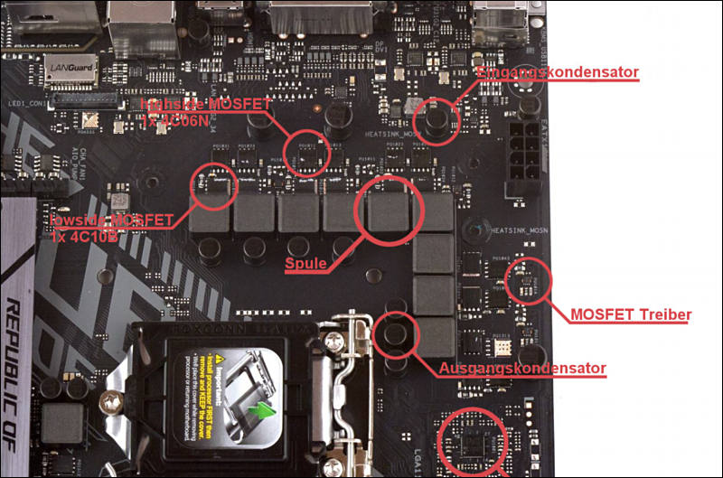
- ASP1400CBT PWM controller
- 4x2 pseudo doubled phases for VCC:
- 1x 4C10B highside MOSFET
- 1x 4C06N lowside MOSFET
- 1 inductor per pseudo phase
- 1 phase for VCCGT:
- 1x 4C10B highside MOSFETs
- 2x 4C06N lowside MOSFETs
- 1 inductor per phase
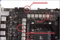
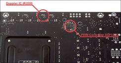
ASUS ROG Crosshair VII Hero
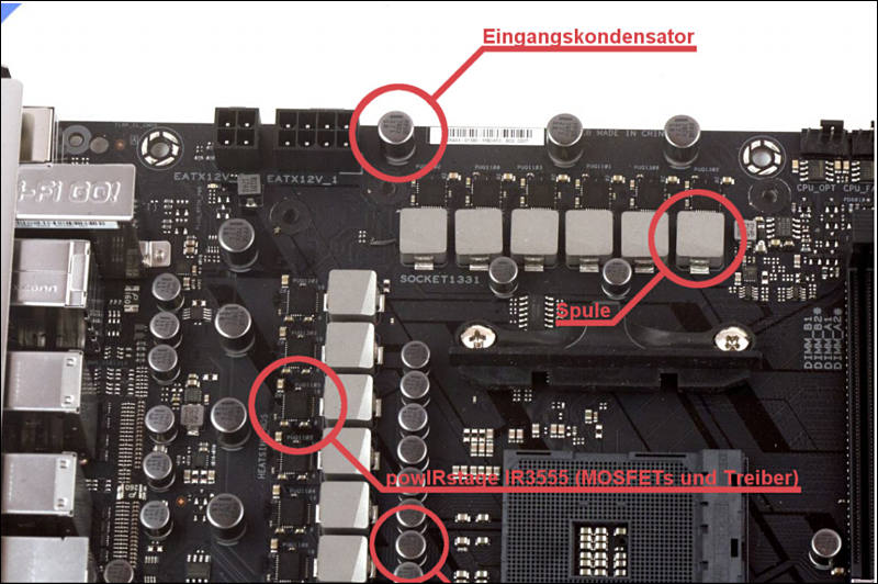
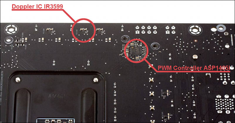
- ASP1405IPWM controller
- 5x2 real doubled phases for CPU VCC:
- IR3599 doublers, one for two phases
- 1x IR3555 powIRstage (has highside MOSFET, lowside MOSFET and driver inside)
- 1 inductor per phase
- 2 phases for SOC VCC:
- 1x IR3555 powIRstage
- 1 inductor per phase
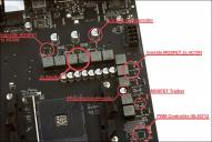
Gigabyte B450 Aorus Pro
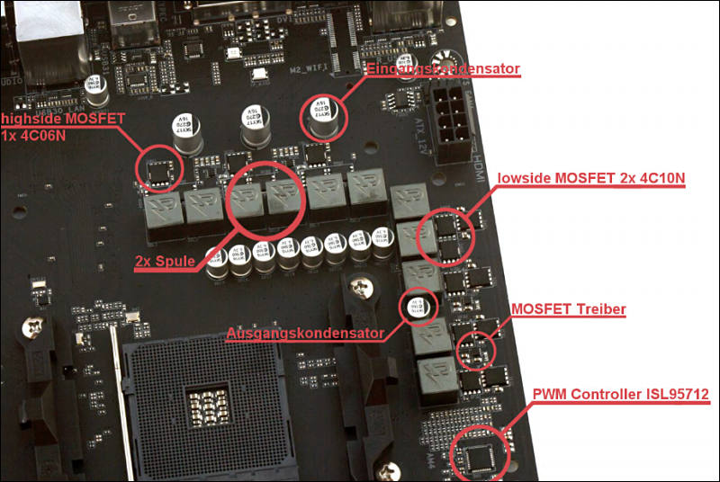
- ISL95712 PWM controller
- 4 phases for CPU VCC:
- 1x 4C10N highside MOSFET
- 2x 4C06N lowside MOSFETs
- 2x inductors per phase (marketing only!)
- 2 phases for SOC:
- 1x 4C10N highside MOSFET
- 1x 4C06N lowside MOSFET
- 1 inductor per phase
 sa6850.jpg800 x 534 - 97K
 sa6852.jpg800 x 529 - 87K
 sa6853.jpg800 x 532 - 85K
 sa6854.jpg800 x 419 - 54K
 sa6855.jpg800 x 536 - 79K
 -
Interesting motherboard sample - ASUS P8P67
PRO and EVO versions are same in this regard
Famous board, and board that sold in big numbers and became famous for sudden problems with VRM.
Made not only by engineering, but also a lot by marketing.
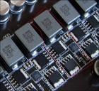
12 + 2 Phase design using PH7030AL and PH5030AL MOSFETs. 12 for CPU VCC and 2 for CPU VTT.
Counting only phases it is same or better than 1-2 highest models in current motherboards lineups (AsRock Taichi has 12 phases for AM4). Yet it is above middle range motherboard.Where is the catch?
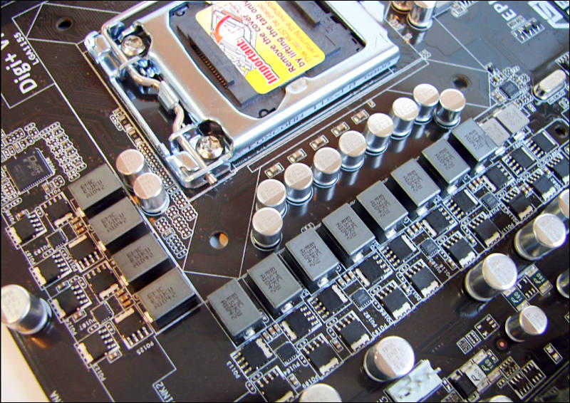
It looks like board uses one high and one low side MOSFET for each phase. Many modern boards use lower number of phases, but doubling of MOSFETs (cheapest double only low side).
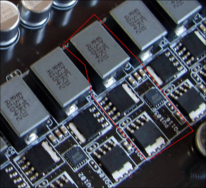
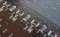
Yet, if we look at other side we can see one more MOSFET per each phase, hidden:
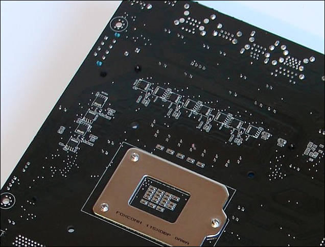
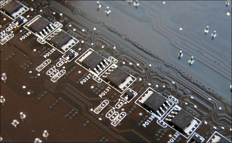
Heatsinks on top are nice.
But hidden below we have MOSFETs that are in the area where air does not move and bad things can happen due to heat.Let's check P8P67 Deluxe
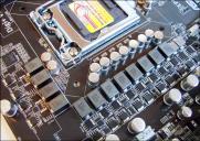
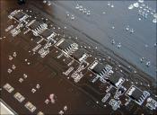
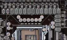
16 + 2 Phase design using. 16 for CPU VCC and 2 for CPU VTT. Same 5030AL MOSFETs.
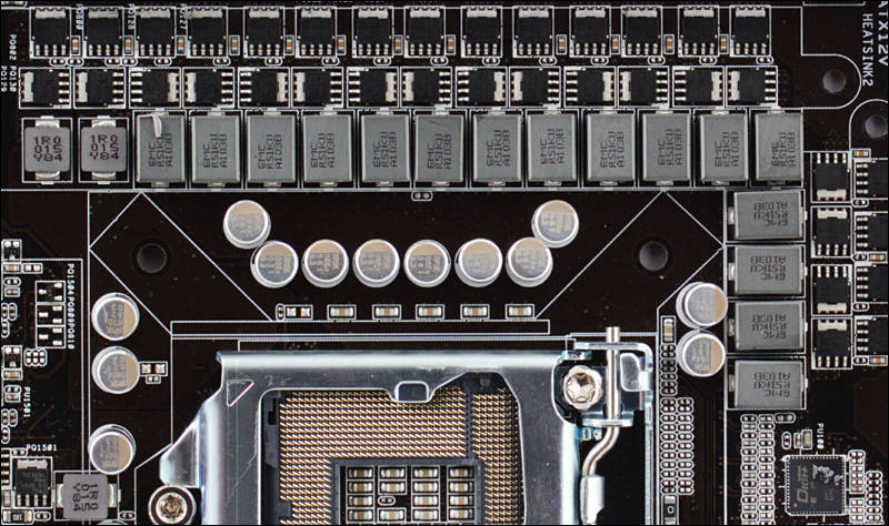
Notice that drivers disappeared.
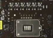
And here they are on the back of the board:
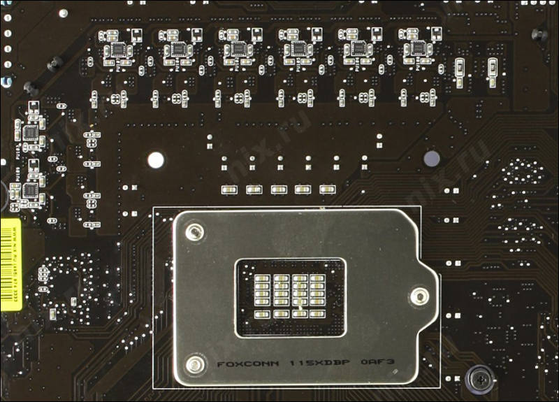
But you no longer notice extra doubling MOSFETs and problem is gone.
Same in the board above - it had been better to use same 2x-4x extra phases and not place hot items where it is hard to cool them.
 sa6864.jpg800 x 566 - 139K
 sa6866.jpg636 x 484 - 54K
 sa6865.jpg800 x 585 - 92K
 sa6867.jpg682 x 622 - 87K
 sa6868.jpg800 x 495 - 80K
 sa6870.jpg800 x 474 - 114K
 sa6869.jpg800 x 575 - 84K
 -
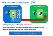
Fully integrated Voltage regulator
Intel in Haswell and Broadwell CPUs did something that was completely new, fully integrate the Voltage regulators of the CPU into the CPU itself, instead of relying on components on the motherboard.
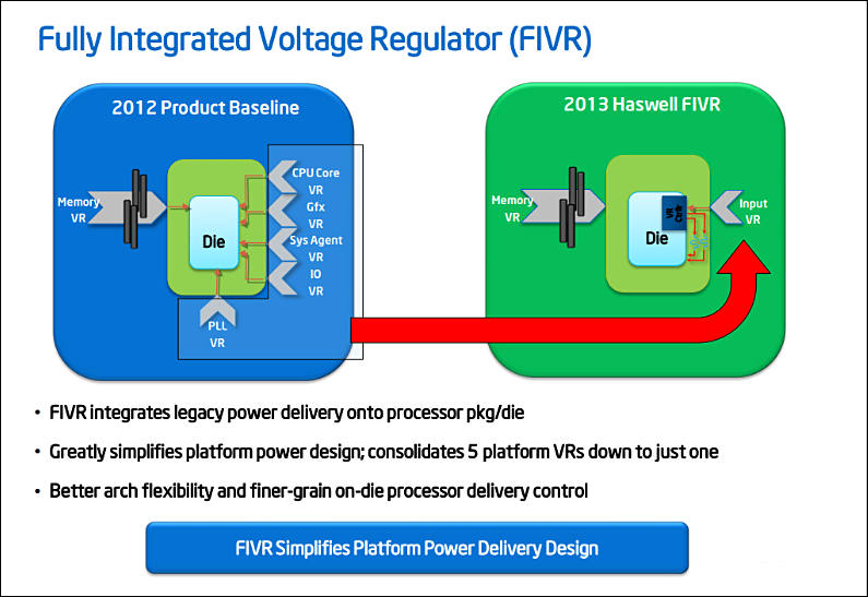
Same thing is present in modern HEDT Skylake-X CPUs and most probably will appear in many new chips.
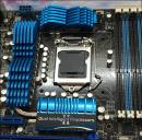
Small comparison of good Sandybridge MOBO
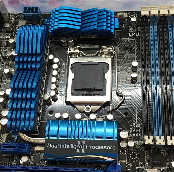
and same good working board for newer Haswell and Broadwell (it is lower end, of course):
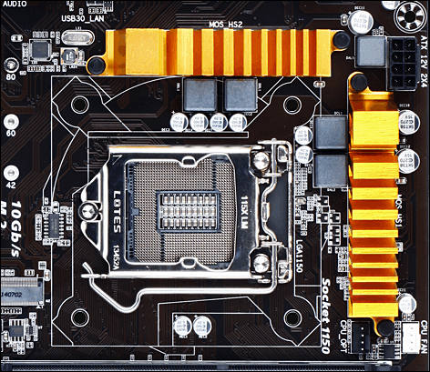
VCCIN runs 1.7-1.9V instead of 1.2-1.4v, so you need around 40% less current.
 sa7256.jpg472 x 409 - 69K
 sa7257.jpg587 x 580 - 111K
 sa7254.jpg795 x 547 - 77K
 -
Useful video
-
VRM Layout Basics and Transient Response
-
What is bad with IR3555?
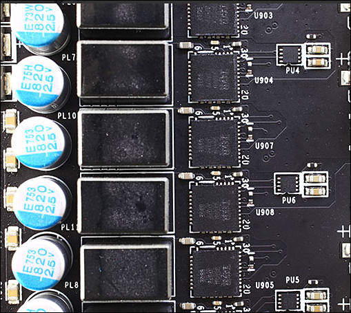
This integrated PowIRstage is very efficient and popular among top motherboards and GPUs, yet it has one issue that reviewers usually miss.
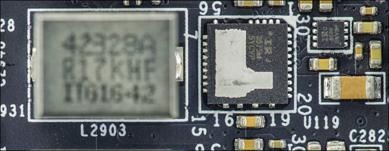
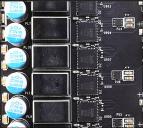
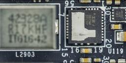
This is how they look on board:
Back of IR3555:
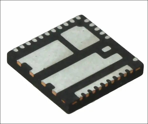
large metal pads are necessary both for high currents and good heat transfer to the motherboard side.
But heat transfer from the top is bad.
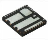
Yet, same company produce IR3575 that fixes such issue
Why we don't see them widely used? Price is around double.
Reason why we still see lot of separate MOSFETs and more stupid and inefficient DrMOS stages lays in the way IR is making big profits.
Main consumption of PowIRstages are servers and similar items, and best of them always consumer IR3575. As all of this products are tightly controlled among quite small number of manufacturers and all have big margins compare to any consumer things - IR also takes some part in it.
 sa9663.jpg509 x 455 - 63K
 sa9662.jpg594 x 497 - 26K
 sa9664.jpg800 x 312 - 53K
Howdy, Stranger!
It looks like you're new here. If you want to get involved, click one of these buttons!
Categories
- Topics List23,992
- Blog5,725
- General and News1,354
- Hacks and Patches1,153
- ↳ Top Settings33
- ↳ Beginners256
- ↳ Archives402
- ↳ Hacks News and Development56
- Cameras2,367
- ↳ Panasonic995
- ↳ Canon118
- ↳ Sony156
- ↳ Nikon96
- ↳ Pentax and Samsung70
- ↳ Olympus and Fujifilm101
- ↳ Compacts and Camcorders300
- ↳ Smartphones for video97
- ↳ Pro Video Cameras191
- ↳ BlackMagic and other raw cameras116
- Skill1,960
- ↳ Business and distribution66
- ↳ Preparation, scripts and legal38
- ↳ Art149
- ↳ Import, Convert, Exporting291
- ↳ Editors191
- ↳ Effects and stunts115
- ↳ Color grading197
- ↳ Sound and Music280
- ↳ Lighting96
- ↳ Software and storage tips266
- Gear5,420
- ↳ Filters, Adapters, Matte boxes344
- ↳ Lenses1,582
- ↳ Follow focus and gears93
- ↳ Sound499
- ↳ Lighting gear314
- ↳ Camera movement230
- ↳ Gimbals and copters302
- ↳ Rigs and related stuff273
- ↳ Power solutions83
- ↳ Monitors and viewfinders340
- ↳ Tripods and fluid heads139
- ↳ Storage286
- ↳ Computers and studio gear560
- ↳ VR and 3D248
- Showcase1,859
- Marketplace2,834
- Offtopic1,320


