It allows to keep PV going, with more focus towards AI, but keeping be one of the few truly independent places.
-
Panasonic Develops Industry’s-First 8K High-Resolution, High-Performance Global Shutter Technology using Organic-Photoconductive-Film CMOS Image Sensor
Osaka Japan, - Panasonic Corporation today announced that it has developed a new technology which realizes 8K high-resolution (36M pixels), 60fps framerate, 450k high-saturation electrons and global shutter [1] imaging with sensitivity modulation function simultaneously, using a CMOS image sensor with an organic photoconductive film (OPF). In this OPF CMOS image sensor, the photoelectric-conversion part and the circuit part are independent. By utilizing this OPF CMOS image sensor's unique structure, we have been able to newly develop and incorporate high-speed noise cancellation technology and high saturation technology in the circuit part. And, by using this OPF CMOS image sensor's unique sensitivity control function to vary the voltage applied to the OPF, we realize global shutter function. The technology that simultaneously achieves these performances is the industry's first*1.
With the technology, it is possible to capture images at 8K resolution, even in high contrast scenes, such as a field under strong sunlight and shaded spectator seats under a stadium roof. Moreover, by utilizing the global shutter function that enables simultaneous image capture by all pixels, it is expected to be able to capture moving objects instantaneously without distortion, be utilized for multi viewpoint cameras (performing multi-view synchronized imaging using plural cameras) and used in fields requiring high-speed and high-resolution, such as machine vision and ITS monitoring. In addition, conventionally, even in scenes where it was necessary to utilize different ND filters [2] according to capturing conditions, the technology realizes a new electronically-controlled variable ND filter function which enables stepless adjustment of the OPF sensitivity [3] merely by controlling the voltage applied to the OPF.
The new technology has the following advantages.
- 8K resolution, 60fps framerate, 450k saturation electrons and global shutter function are realized simultaneously.
- Switching between high sensitivity mode and high saturation mode is possible using gain switching function.
- The ND filter function can be realized steplessly by controlling the voltage applied to the OPF.
This Development is based on the following technologies
- "OPF CMOS image sensor design technology", in that, the photoelectric-conversion part and the circuit part can be designed independently.
- "In-pixel capacitive coupled noise cancellation technique" which can suppress pixel reset noise at high speed even at high resolution
- "In-pixel gain switching technology" that can achieve high saturation characteristics
- "Voltage controlled sensitivity modulation technology" that can adjust the sensitivity by changing the voltage applied to the OPF.
Panasonic holds 135 Japanese patents and 83 overseas patents (including pending) related to this technology.
Panasonic will present some of these technologies at the international academic conference: ISSCC (International Solid-State Circuit Conference) 2018 which will be held in San Francisco on February 11 - 15, 2018.
More on the Technology
"OPF CMOS image sensor design technology", in that, the photoelectric-conversion part and the circuit part can be designed independently.
The OPF CMOS image sensor has a unique structure, in which, the OPF performs a photoelectric conversion and the circuit area performs charge storage and signal readout functions completely independently. Using this OPF CMOS image sensor structure, we developed high-speed noise cancellation technology and high saturation technology in the circuit area which has a large available space. As a result, it is possible to realize simultaneously 8K resolution, 60fps framerate readout, wide dynamic range [4] (by achieving a high saturation level) and global shutter function, which are normally traded off.


"In-pixel capacitive coupled noise cancellation technique" which can suppress pixel reset noise at high speed even at high resolution
Because the OPF CMOS image sensor has a structure in which the OPF and the charge storage part are connected by metal plugs, accumulated charges cannot be completely read out. Therefore, there is a problem that it is affected by reset noise at the time of resetting the pixel (signal charge storage node). And, in a high-resolution sensor, such as an 8K sensor, it is necessary to drive large loads exceeding 4000 pixels aligned in the vertical direction at the same time as the time of noise cancellation, and therefore, the long time it takes to suppress noise is a problem. So, we developed a new structure that cancels pixel reset noise at high speed, even when high resolution pixels have to be driven, by using Panasonic's original semiconductor device technology and the newly developed "in-pixel capacitive coupled noise canceller". In this structure, the reset noise is suppressed at high speed by using the negative feedback loop provided for each pixel.

"In-pixel gain switching technology" that can achieve high saturation characteristics
In the OPF CMOS image sensor, by incorporating a large capacitor in the circuit part with a large available area, it is possible to realize both high sensitivity mode and high saturation mode with the same pixel structure merely by switching modes from the camera system. In the high sensitivity mode, it is possible to capture data up to a light intensity of 4.5k electrons with high sensitivity. Furthermore, by switching to the high saturation mode, it is possible to capture data up to a light intensity of 450k electrons. In this way, since the high saturation mode can capture up to 10 times the high sensitivity mode, it is possible to clearly display the fine winding structure of the lamp filaments, in which bright part gradation cannot be expressed, because it becomes overexposure in high sensitivity mode, as shown in Fig. 3 (a). Even in a scene with high contrast, such as shown in Fig. 5, from the facial expression of the person in the shadow of the stadium roof to the blue sky and clouds during a mid-summer day, and such as shown in Fig. 6, from the dimly lit room to the sunny garden, it will be possible to capture brilliant images without overexposure or underexposure.

"Voltage controlled sensitivity modulation technology" that can adjust the sensitivity by changing the voltage applied to the OPF.
The OPF CMOS image sensor can change the sensitivity of the OPF simply by controlling the voltage applied to the OPF. By utilizing this function, we can realize the following functions which could not be realized with conventional silicon image sensors.
Sensitivity Modulation Example 1: Global shutter function which can capture all pixels simultaneously at 8K resolution
By controlling ON / OFF of the voltage applied to the OPF and controlling the sensitivity of the OPF, we realize the "global shutter function" capable of imaging all pixels at the same time, even driving a large number of pixels like the 8K sensor. By capturing with the global shutter function, as shown in Fig. 3 (b), the letters on the rotating body are read sharply without distortion. In addition, as shown in Fig. 7, even at the time of high speed moving object capturing, such as when driving on a highway or at industrial inspection, capturing without distortion becomes possible.

In the conventional global shutter type silicon image sensor, it is necessary to add new elements such as transfer circuits and charge storage capacitors in order to accumulate charges simultaneously in all pixels. As a result, the area of the photodiode and that of the additional circuits must compete for space, there is a problem that the pixel size cannot be reduced and the amount of saturation electrons cannot be increased. On the other hand, in the OPF CMOS image sensor, since there is no need for additional elements, it is possible to realize small cell, high resolution sensors, and by incorporating large capacitors in the circuit part with a large available area, accurate imaging with no distortion from dark scenes to extremely bright scenes is possible. For example, as shown in Fig. 9, with the OPF CMOS image sensor, when buildings are photographed while panning [5] at high speed, even in scenes with high contrast like a bright sky and dark windows, it is possible to acquire image data maintaining all gradations of the whole area without distortion.

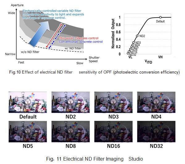
Sensitivity Modulation Example 2: "Electrical ND Filter Technology" which can change sensitivity continuously and steplessly
Conventionally it has been necessary to provide a plurality of ND filters according to photographing conditions and change them many times. On the other hand, in the OPF CMOS image sensor, merely by controlling the voltage applied to the OPF (VITO in Fig. 8) and changing the sensitivity of the OPF to the desired value, it is possible to electrically implement the ND filter function. By using this function, it becomes possible to simplify the photographic equipment and continuously, steplessly control the sensitivity which could not be realized with a conventional silicon sensor. Therefore, the possibility of capturing according to the scene is expanded.
In the future, we will utilize this OPF CMOS image sensor technology in various applications such as broadcasting cameras, surveillance cameras, industrial inspection cameras, automotive cameras, etc., and will contribute to realize high resolution, high speed and high precision imaging and sensing functions.
-
Thanks for post, I put original Panasonic PR, instead of damaged version without formatting made by 43rumors.
-
Opinion about this sensor
Nishimura of Panasonic talked about the organic-photoconductive film GS CIS with an in-pixel noise canceller. It is not the first time that this technology is presented at ISSCC, but this time an extra noise cancellation “trick” is applied in the pixel to lower the noise. Do not forget that this pixel is basically a 3T pixel that suffers from kTC noise. A similar noise cancellation method was applied as what we have seen earlier with the so-called “active reset”, but no longer on column level, this time on pixel level. Key advantage of this device is the GS mode with very good PLS (- 110 dB), tunable sensitivity by biasing the right voltage across the photoconductor, very high saturation level. The paper claims that the reset noise is lowered by a factor of 10, while the saturation level is increased by a factor of 10 (but the high saturation mode cannot be combined with the low noise level). The pixel size is 3 um x 3 um, for a 8192 x 4320 pixels, 60 fps, 12 bit ADC, 65 nm process technology 1P4Cu1Al, noise of 8.6 e (in the proceedings, not consistent with the presentation where it was mentioned 4.5 e). But again not a single indication about dark current and dark non-uniformities. During the presentation as well as after the session, super quality images were shown, but all was prerecorded.
-
With the technology, it is possible to capture images at 8K resolution, even in high contrast scenes, such as a field under strong sunlight and shaded spectator seats under a stadium roof. Moreover, by utilizing the global shutter function that enables simultaneous image capture by all pixels, it is expected to be able to capture moving objects instantaneously without distortion, be utilized for multi viewpoint cameras (performing multi-view synchronized imaging using plural cameras) and used in fields requiring high-speed and high-resolution, such as machine vision and ITS monitoring. In addition, conventionally, even in scenes where it was necessary to utilize different ND filters [2] according to capturing conditions, the technology realizes a new electronically-controlled variable ND filter function which enables stepless adjustment of the OPF sensitivity [3] merely by controlling the voltage applied to the OPF.
This interests me even more than the 8K
The ND filter function can be realized steplessly by controlling the voltage applied to the OPF.
-
For now it is research paper and few sensors made in lab.
-
Any use in a GH6 or what ever is probably very far off if ever. I remember reading a comment that the organic sensor runs hot and is power hungry which would make it it a problem in a small body for sure. That being said I wish them the best it sounds wonderful. At this point it's good PR but nothing more.
-
I thought it was a dead project. Good to see its all good. The las time I thought fujifilm was involved.
Is very good PR and R&D. I wish them the best. 2020 maybe we will se implementation in Olympics as they aim 8k that year in all Japan.
Either way, we are seeing a very good advance in sensor evolution. I am very interested in the lythographic process of this organic sensor. What substrate is used as organic compound etc.
-
"The pixel size is 3 um x 3 um, for a 8192 x 4320"
That works out to a sensor size of approx 24.5 x 13mm which is a 35mm 3-perf frame. Not likely going into a micro 4/3 camera. I can just see them releasing this next generation camera with an EF lens mount. :(
-
They did it! This is a dream coming true.
Everything we hate in silicon is solved.
-
@apefos there is always trade offs first we have nothing commercial yet and organic has it's own set of issues. Basically good news but keep the champagne on ice.
@endotoxic Fujifilm and others are still involved I believe there is a group. Here is a article you night find interesting https://www.fujirumors.com/fujifilm-announces-development-worlds-fastest-organic-cmos-circuit-multi-bit-flexible-temperature-sensor/
-
Woops wrong place
-
@Apefos black silicon and graphene are two materials that are available but long off the race track compared to organic sensor. Yes we are at the verge of leaving silicon, but still much time is needed to achieve that.


Howdy, Stranger!
It looks like you're new here. If you want to get involved, click one of these buttons!
Categories
- Topics List23,992
- Blog5,725
- General and News1,354
- Hacks and Patches1,153
- ↳ Top Settings33
- ↳ Beginners256
- ↳ Archives402
- ↳ Hacks News and Development56
- Cameras2,367
- ↳ Panasonic995
- ↳ Canon118
- ↳ Sony156
- ↳ Nikon96
- ↳ Pentax and Samsung70
- ↳ Olympus and Fujifilm101
- ↳ Compacts and Camcorders300
- ↳ Smartphones for video97
- ↳ Pro Video Cameras191
- ↳ BlackMagic and other raw cameras116
- Skill1,960
- ↳ Business and distribution66
- ↳ Preparation, scripts and legal38
- ↳ Art149
- ↳ Import, Convert, Exporting291
- ↳ Editors191
- ↳ Effects and stunts115
- ↳ Color grading197
- ↳ Sound and Music280
- ↳ Lighting96
- ↳ Software and storage tips266
- Gear5,420
- ↳ Filters, Adapters, Matte boxes344
- ↳ Lenses1,582
- ↳ Follow focus and gears93
- ↳ Sound499
- ↳ Lighting gear314
- ↳ Camera movement230
- ↳ Gimbals and copters302
- ↳ Rigs and related stuff273
- ↳ Power solutions83
- ↳ Monitors and viewfinders340
- ↳ Tripods and fluid heads139
- ↳ Storage286
- ↳ Computers and studio gear560
- ↳ VR and 3D248
- Showcase1,859
- Marketplace2,834
- Offtopic1,320


