It allows to keep PV going, with more focus towards AI, but keeping be one of the few truly independent places.
-
Sony Corporation today announced that it has developed a 1.46 effective megapixel back-illuminated CMOS image sensor equipped with a Global Shutter function*1. The newly developed pixel-parallel analog-to-digital converters provide the function to instantly convert the analog signal from all pixels, simultaneously exposed, to a digital signal in parallel. This new technology was announced at the International Solid-State Circuits Conference (ISSCC) on February 11, 2018 in San Francisco in the United States.
CMOS image sensors using the conventional column A/D conversion method read out the photoelectrically converted analog signals from pixels row by row, which results in image distortion (focal plane distortion) caused by the time shift due to the row-by-row readout.
The new Sony sensor comes with newly developed low-current, compact A/D converters positioned beneath each pixel. These A/D converters instantly convert the analog signal from all the simultaneously exposed pixels in parallel to a digital signal to temporarily store it in digital memory. This architecture eliminates focal plane distortion due to readout time shift, making it possible to provide a Global Shutter function1, an industry-first for a high-sensitivity back-illuminated CMOS sensor with pixel-parallel A/D Converter with more than one megapixel3.
The inclusion of nearly 1,000 times as many A/D converters compared to the traditional column A/D conversion method2 means an increased demand for current. Sony addressed this issue by developing a compact 14-bit A/D converter which boasts the industry’s best performance4 in low-current operation.
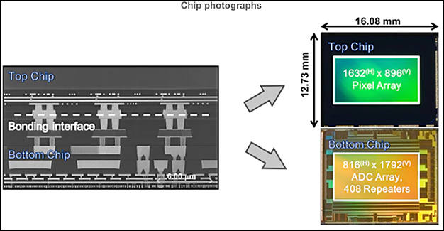
Both the A/D converter and digital memory spaces are secured in a stacked configuration with these elements integrated into the bottom chip. The connection between each pixel on the top chip uses Cu-Cu (copper-copper) connection*5, a technology that Sony put into mass production as a world-first in January 2016.
In addition, a newly developed data transfer mechanism is implemented into the sensor to enable the high-speed massively parallel readout data required for the A/D conversion process.
Main Features
Global Shutter function achieved in a high-sensitivity back-illuminated CMOS image sensor by using the following key technologies: Low-current, compact pixel-parallel A/D converter. In order to curtail power consumption, the new converter uses comparators that operate with subthreshold currents, resulting in the industry’s best-performing4, low current, compact 14-bit A/D converter. This overcomes the issue of the increased demand for current due to the inclusion of nearly 1,000 times as many A/D converters in comparison with the traditional column A/D conversion method2.
Cu-Cu (copper-copper) connection
To achieve the parallel A/D conversion for all pixels, Sony has developed a technology which makes it possible to include approximately three million Cu-Cu (copper-copper) connections*5 in one sensor. The Cu-Cu connection provides electrical continuity between the pixel and logic substrate, while securing space for implementing as many as 1.46 million A/D converters, the same number as the effective megapixels, as well as the digital memory.High-speed data transfer construction
Sony has developed a new readout circuit to support the massively parallel digital signal transfer required in the A/D conversion process using 1.46 million A/D converters, making it possible to read and write all the pixel signals at high speed. sa1731.jpg626 x 325 - 38K
 -
Opinion about it
Sakakibara (Sony) presented a paper about a BSI-GS CMOS imager with pixel-parallel 14b ADC. One can make a global shutter in a CMOS sensor in the charge domain, in the voltage domain, but also in the digital domain. The latter requires an ADC per pixel (also known as DPS : digital pixel sensor). And this paper describes such a solution : a stacked image sensor with per pixel a single ADC. Based on the recent history of Sony technology, it could be expected that this technology was coming. The ADC (per pixel !) is a single slope ADC with a comparator and a latch per pixel. The design of the pixel is such that the source follower is already part of the comparator. That makes the structure very compact, but requires two Cu-Cu contacts between top and bottom layer per pixel. To get rid of all the data generated by all these ADCs, a pretty complex data line structure is implemented. The technologies used : 90 nm 1P4M for the top layer, 65 nm 1P7M for the bottom layer. Pixel size is 6.9 um x 6.9 um, 1.46 Mpixels, noise level 5.15 e in a high power mode of 746 mW @ 660 fps or 8.77 e in a low power mode of 654 mW @ 660 fps. Dynamic range for the two modes is respectively 70.2 dB and 65.7 dB. PLS for this global shutter is -75 dB.


Howdy, Stranger!
It looks like you're new here. If you want to get involved, click one of these buttons!
Categories
- Topics List23,991
- Blog5,725
- General and News1,354
- Hacks and Patches1,153
- ↳ Top Settings33
- ↳ Beginners256
- ↳ Archives402
- ↳ Hacks News and Development56
- Cameras2,367
- ↳ Panasonic995
- ↳ Canon118
- ↳ Sony156
- ↳ Nikon96
- ↳ Pentax and Samsung70
- ↳ Olympus and Fujifilm101
- ↳ Compacts and Camcorders300
- ↳ Smartphones for video97
- ↳ Pro Video Cameras191
- ↳ BlackMagic and other raw cameras116
- Skill1,960
- ↳ Business and distribution66
- ↳ Preparation, scripts and legal38
- ↳ Art149
- ↳ Import, Convert, Exporting291
- ↳ Editors191
- ↳ Effects and stunts115
- ↳ Color grading197
- ↳ Sound and Music280
- ↳ Lighting96
- ↳ Software and storage tips266
- Gear5,420
- ↳ Filters, Adapters, Matte boxes344
- ↳ Lenses1,582
- ↳ Follow focus and gears93
- ↳ Sound499
- ↳ Lighting gear314
- ↳ Camera movement230
- ↳ Gimbals and copters302
- ↳ Rigs and related stuff273
- ↳ Power solutions83
- ↳ Monitors and viewfinders340
- ↳ Tripods and fluid heads139
- ↳ Storage286
- ↳ Computers and studio gear560
- ↳ VR and 3D248
- Showcase1,859
- Marketplace2,834
- Offtopic1,319


