It allows to keep PV going, with more focus towards AI, but keeping be one of the few truly independent places.
-
SK Hynix plans to launch the mass-production of 48-stack 3D NAND flash memory chips from the end of this month. This is the second time among global memory chip makers to do so behind Samsung Electronics.
In a situation where the flat micro-processing technology reached its limit at around 10 nanometers, 3D NAND was developed as an alternative to overcome the limit.
SK Hynix will increase its monthly 3D NAND output from 10,000 units in the third quarter of last year to 20,000-30,000 units by the end of this year, with the share of 3D NAND in its overall NAND output rising to around 15 percent.
The share of 3D NAND in NAND companies' overall production is forecast to rise to 57.8 percent in 2017 from 23.6 percent in 2016 and 6.7 percent in 2015.
SK Hynix is now developing the next-generation 72-stack 3D NAND and is expected to begin the mass-production from the latter half of next year.
Note that it is almost all TLC memory, not only it can have speed issues http://www.personal-view.com/talks/discussion/15972/tlc-and-mlc-difference-in-cheap-ssds#Item_2 but rewrite cycles are lower and lower.
Today's commodity 2D MLC flash has raw wear-out in the 2,000 to 3,000 write cycle range.
Samsung TLC specs at 1000 cycles.
2D QLC (4 bit one) memory must drop to 500 cycles.
-
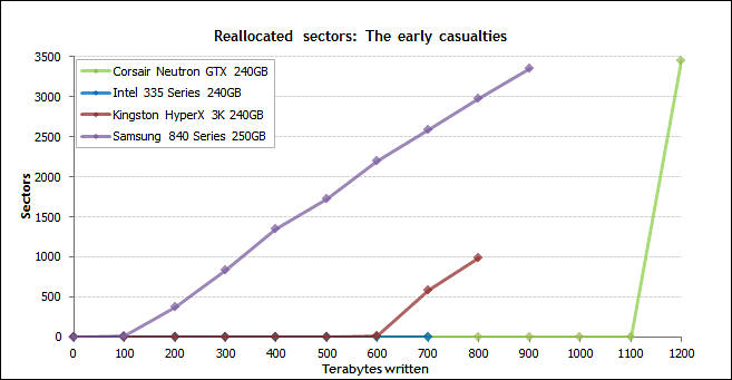
Samsung is very optimistic, but not all agree with this.
http://techreport.com/review/27909/the-ssd-endurance-experiment-theyre-all-dead
 img2870.jpg657 x 341 - 38K


Howdy, Stranger!
It looks like you're new here. If you want to get involved, click one of these buttons!
Categories
- Topics List23,985
- Blog5,725
- General and News1,353
- Hacks and Patches1,152
- ↳ Top Settings33
- ↳ Beginners255
- ↳ Archives402
- ↳ Hacks News and Development56
- Cameras2,363
- ↳ Panasonic993
- ↳ Canon118
- ↳ Sony156
- ↳ Nikon96
- ↳ Pentax and Samsung70
- ↳ Olympus and Fujifilm100
- ↳ Compacts and Camcorders300
- ↳ Smartphones for video97
- ↳ Pro Video Cameras191
- ↳ BlackMagic and other raw cameras115
- Skill1,960
- ↳ Business and distribution66
- ↳ Preparation, scripts and legal38
- ↳ Art149
- ↳ Import, Convert, Exporting291
- ↳ Editors191
- ↳ Effects and stunts115
- ↳ Color grading197
- ↳ Sound and Music280
- ↳ Lighting96
- ↳ Software and storage tips266
- Gear5,420
- ↳ Filters, Adapters, Matte boxes344
- ↳ Lenses1,582
- ↳ Follow focus and gears93
- ↳ Sound499
- ↳ Lighting gear314
- ↳ Camera movement230
- ↳ Gimbals and copters302
- ↳ Rigs and related stuff273
- ↳ Power solutions83
- ↳ Monitors and viewfinders340
- ↳ Tripods and fluid heads139
- ↳ Storage286
- ↳ Computers and studio gear560
- ↳ VR and 3D248
- Showcase1,859
- Marketplace2,834
- Offtopic1,319


