Please, support PV!
It allows to keep PV going, with more focus towards AI, but keeping be one of the few truly independent places.
It allows to keep PV going, with more focus towards AI, but keeping be one of the few truly independent places.
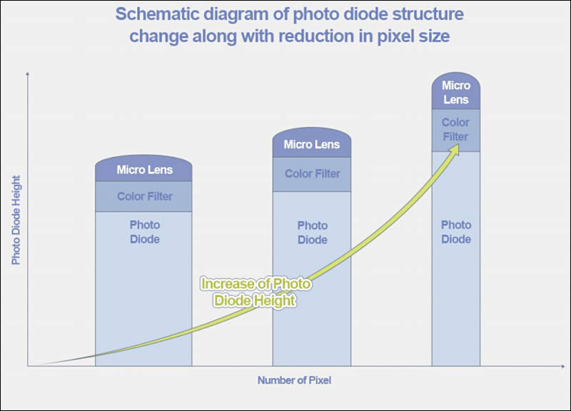
Photo diode structure change in small modern sensors
-

The pixel size should be more reduced to increase the number of pixels in the same chip size. Also, forming deep PD is a key technology to avoid deterioration in image quality. To secure sufficient full well capacity (FWC) in small pixels, patterning and implementing technologies with higher difficulty level compared to the ones for semiconductor memory are required. Especially, it is essential to secure a high aspect ratio (>15:1) implant MASK process technology that can block high-energy ion implantation; in fact, the aspect ratio tends to be gradually increasing in the industry these days.

 sa15818.jpg800 x 576 - 44K
Start New Topic


Howdy, Stranger!
It looks like you're new here. If you want to get involved, click one of these buttons!
Categories
- Topics List23,992
- Blog5,725
- General and News1,354
- Hacks and Patches1,153
- ↳ Top Settings33
- ↳ Beginners256
- ↳ Archives402
- ↳ Hacks News and Development56
- Cameras2,367
- ↳ Panasonic995
- ↳ Canon118
- ↳ Sony156
- ↳ Nikon96
- ↳ Pentax and Samsung70
- ↳ Olympus and Fujifilm101
- ↳ Compacts and Camcorders300
- ↳ Smartphones for video97
- ↳ Pro Video Cameras191
- ↳ BlackMagic and other raw cameras116
- Skill1,960
- ↳ Business and distribution66
- ↳ Preparation, scripts and legal38
- ↳ Art149
- ↳ Import, Convert, Exporting291
- ↳ Editors191
- ↳ Effects and stunts115
- ↳ Color grading197
- ↳ Sound and Music280
- ↳ Lighting96
- ↳ Software and storage tips266
- Gear5,420
- ↳ Filters, Adapters, Matte boxes344
- ↳ Lenses1,582
- ↳ Follow focus and gears93
- ↳ Sound499
- ↳ Lighting gear314
- ↳ Camera movement230
- ↳ Gimbals and copters302
- ↳ Rigs and related stuff273
- ↳ Power solutions83
- ↳ Monitors and viewfinders340
- ↳ Tripods and fluid heads139
- ↳ Storage286
- ↳ Computers and studio gear560
- ↳ VR and 3D248
- Showcase1,859
- Marketplace2,834
- Offtopic1,320


