-

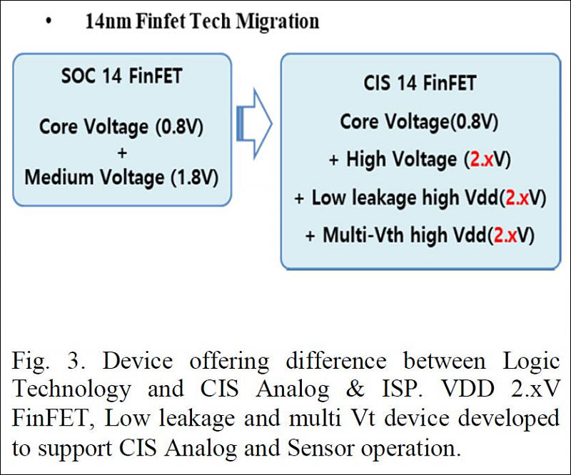
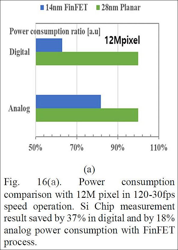
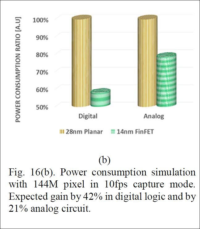
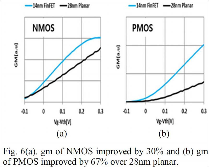
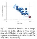
CMOS Image Sensor(CIS) products need higher voltage device and better analog characteristics than conventional SOC & Logic products. This work presents newly developed 14nm FinFET process with 2.xV high voltage FinFET device characteristics showing excellent analog and low power digital characteristics comparing to 28nm planar process. Gm is improved by 30% and 67% in FinFET process for NMOS and PMOS, respectively. Rout characteristics increased by 40 times and 6 times over 28nm planar process. Interface state density(Nit) improved by more than 40% and flicker noise characteristics also improved by 64% and 42% for NMOS and PMOS, respectively. Digital logic Transistor ion-ioff performance improved by by 32% and by 211% for NMOS and PMOS, respectively compared to 28nm planar device and the chip power consumption of digital logic functional block reduced by 34% in real Si of 12M pixel product. 14nm FinFET process expected to improve power consumption by 42% in 144M pixel density.
 sa11483.jpg684 x 726 - 72K
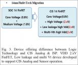 sa11484.jpg800 x 666 - 83K
 sa11485.jpg592 x 828 - 75K
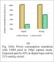 sa11486.jpg648 x 744 - 64K
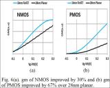 sa11487.jpg800 x 642 - 61K


Howdy, Stranger!
It looks like you're new here. If you want to get involved, click one of these buttons!
Categories
- Topics List23,965
- Blog5,723
- General and News1,343
- Hacks and Patches1,151
- ↳ Top Settings33
- ↳ Beginners254
- ↳ Archives402
- ↳ Hacks News and Development56
- Cameras2,361
- ↳ Panasonic990
- ↳ Canon118
- ↳ Sony154
- ↳ Nikon96
- ↳ Pentax and Samsung70
- ↳ Olympus and Fujifilm99
- ↳ Compacts and Camcorders299
- ↳ Smartphones for video97
- ↳ Pro Video Cameras191
- ↳ BlackMagic and other raw cameras121
- Skill1,961
- ↳ Business and distribution66
- ↳ Preparation, scripts and legal38
- ↳ Art149
- ↳ Import, Convert, Exporting291
- ↳ Editors191
- ↳ Effects and stunts115
- ↳ Color grading197
- ↳ Sound and Music280
- ↳ Lighting96
- ↳ Software and storage tips267
- Gear5,414
- ↳ Filters, Adapters, Matte boxes344
- ↳ Lenses1,579
- ↳ Follow focus and gears93
- ↳ Sound498
- ↳ Lighting gear314
- ↳ Camera movement230
- ↳ Gimbals and copters302
- ↳ Rigs and related stuff272
- ↳ Power solutions83
- ↳ Monitors and viewfinders339
- ↳ Tripods and fluid heads139
- ↳ Storage286
- ↳ Computers and studio gear560
- ↳ VR and 3D248
- Showcase1,859
- Marketplace2,834
- Offtopic1,319


