It allows to keep PV going, with more focus towards AI, but keeping be one of the few truly independent places.
-
TSMC has obtained orders for CMOS image sensors from Sony, and will fabricate the chips using 40nm process technology at Fab 14A in Tainan, southern Taiwan, according to a recent Chinese-language Commercial Times report.
TSMC has placed equipment orders for additional 40nm process capacity at the fab in order to fulfill Sony's orders for CIS, said the report, without citing its source. The foundry is scheduled to install the additional new 40nm manufacturing equipment in the second quarter of 2020 with pilot runs slated for August next year.
Relations is Sony-Samsung cartel are deteriorating quite fast due to quickly rising Samsung capacity and possible final fight that can happen in the late 2021-2022. Sony such way needs to manufacture more sensors in the safe place.
We can see huge and brutal fight where only one will survive and 98% it won't be Sony.
-
United Microelectronics (UMC), through its takeover of Mie Fujitsu Semiconductor (MIFS), has entered the supply chain for Sony's CMOS image sensors.
Safety first.
-
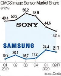
According to market researcher OMDIA, the global market share gap in the CMOS image sensor between Sony and Samsung has narrowed significantly this year.
Sony’s global market share, which rose to as high as 56.2% in the third quarter of 2019, fell to an estimated 42.5% in the second quarter of 2020.
In the same period, the market share of Samsung, the world’s No. 2 image sensor maker, rose to 21.7% from 16.7%, narrowing the gap with the Japanese company to 20.8 percentage points from 39.5 percentage points.
Analysts attribute Samsung’s advancement in the image sensor market to the increase in shipments of its high-end products and a growing client base such as Chinse electronics firm Xiaomi Corp.
It is very dangerous for Sony, especially with so bad dedicated cameras market. They no longer can try some of advanhed techniques almost for free, as they had all financed by rich professionals or tourists.
 sa14003.jpg202 x 252 - 13K
 -
It is dangerous for Sony
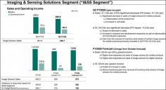
Sony’s image sensor sales are predicted to fall from 240 billion yen in the second quarter of this year to 130 billion yen in the second quarter of next year.
This is leading to an opportunity for Samsung. The latecomer in the industry has focused on Xiaomi, Vivo and others rather than Huawei.
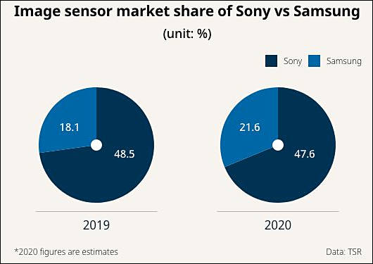
Samsung is aiming to rise to the top in the global image sensor market by 2030. Last year, Samsung’ share in the market was 18.1 percent and Sony’s was 53.5 percen
-
 sa15814.jpg567 x 351 - 22K
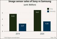 sa15815.jpg542 x 368 - 25K
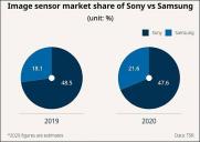 sa15816.jpg530 x 375 - 26K
 -
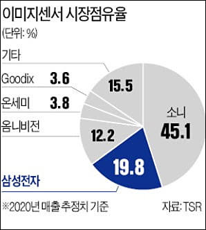
Info from TSR market report:
- In 2020, Sony market share was 45.1%, Samsung's - 19.8%
- Gap shrunk by 5.1-5.2% in comparison with 2019
- TSR expects this gap to shrink further to 10% in 2021
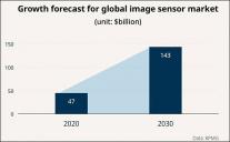
- The global image sensor market is forecasted to increase by 22.1% from $20.4B this year to $24.9B in 2024
- The global image sensor market is forecasted to increase by 11.4% annually from $17.9B this year to $24.8B in 2024
 sa16606.jpg298 x 332 - 18K
 -
Sony buys patents
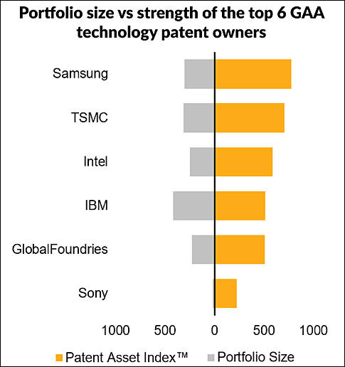
"The respective reassignment document lists 35 simple patent families with active US patents. Looking at the drawings shows that the portfolio comprises various technologies like packaging, semiconductor process, systems, computer memory, and image projection. Surprisingly, there are several first page drawings which points to gate-all-around transistor (GAA) technologies, the expected next transistors technology.
This finding was not expected: Sony is not known to be active in advanced CMOS transistor technologies like GAA, or at least not obviously known.
...a quick screening shows that 10 patent families are about to gate-all-around transistors and 3 families relate to finFET transistors. On its face value, the described structures and methods even resemble gate-all-around structures which are published in the literature.
Sony ranks sixth with a small but strong GAA portfolio. Difference between the portfolio size (number of simple patent families) and the portfolio strength (Patent Asset Index) is remarkable: The portfolio strength is more than 10-times larger than the Portfolio Size. This ratio demonstrates the high average quality, measured by the PatentSight Competitive Impact, of Sony's gate-all-around patents, as the Patent Asset Index is the product of Competitive Impact and Portfolio Size.
 sa16706.jpg485 x 516 - 31K
 -
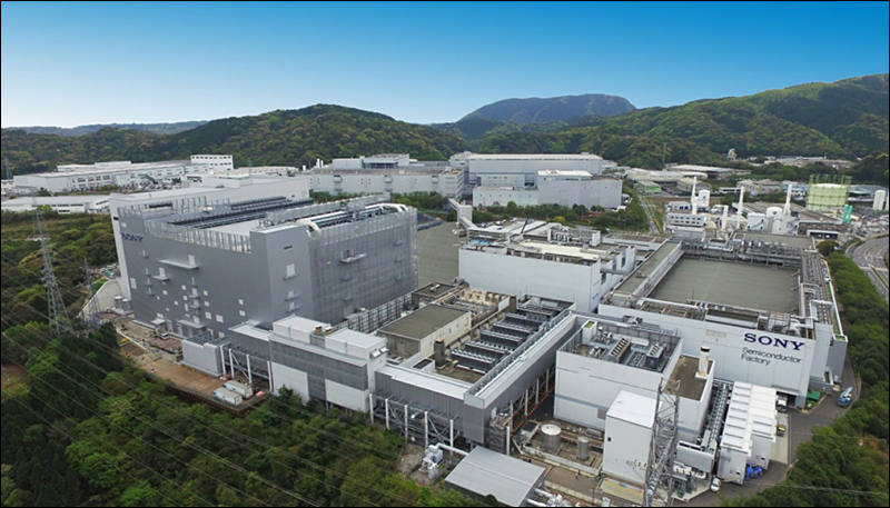
Sony Semiconductor Solutions announces that, starting in April 2021, it has begun operations on the production lines at the new fab built on the premises of Nagasaki Technology Center (“Nagasaki TEC”), a production center owned by Sony Semiconductor Manufacturing Corporation. The new fab, dubbed “Fab 5,” will be utilized for the mass production of CMOS sensors.
 sa17043.jpg800 x 457 - 76K


Howdy, Stranger!
It looks like you're new here. If you want to get involved, click one of these buttons!
Categories
- Topics List23,992
- Blog5,725
- General and News1,354
- Hacks and Patches1,153
- ↳ Top Settings33
- ↳ Beginners256
- ↳ Archives402
- ↳ Hacks News and Development56
- Cameras2,367
- ↳ Panasonic995
- ↳ Canon118
- ↳ Sony156
- ↳ Nikon96
- ↳ Pentax and Samsung70
- ↳ Olympus and Fujifilm101
- ↳ Compacts and Camcorders300
- ↳ Smartphones for video97
- ↳ Pro Video Cameras191
- ↳ BlackMagic and other raw cameras116
- Skill1,960
- ↳ Business and distribution66
- ↳ Preparation, scripts and legal38
- ↳ Art149
- ↳ Import, Convert, Exporting291
- ↳ Editors191
- ↳ Effects and stunts115
- ↳ Color grading197
- ↳ Sound and Music280
- ↳ Lighting96
- ↳ Software and storage tips266
- Gear5,420
- ↳ Filters, Adapters, Matte boxes344
- ↳ Lenses1,582
- ↳ Follow focus and gears93
- ↳ Sound499
- ↳ Lighting gear314
- ↳ Camera movement230
- ↳ Gimbals and copters302
- ↳ Rigs and related stuff273
- ↳ Power solutions83
- ↳ Monitors and viewfinders340
- ↳ Tripods and fluid heads139
- ↳ Storage286
- ↳ Computers and studio gear560
- ↳ VR and 3D248
- Showcase1,859
- Marketplace2,834
- Offtopic1,320


