It allows to keep PV going, with more focus towards AI, but keeping be one of the few truly independent places.
-
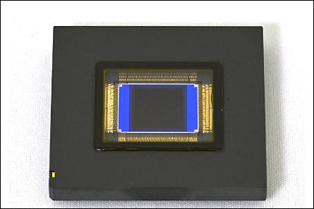
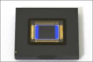
Nikon Corporation (Nikon) has developed a stacked, 4K × 4K, CMOS image sensor with a total pixel count of approximately 17.8 megapixels that realizes high-resolution imaging with 1000 frames per second, and high dynamic range (HDR) characteristics of 110 dB.
- Manufacturing process 65 nm BSI + 65 nm CMOS Wafer level stacking process
- Image sensor 1-inch CMOS image sensor
- Pixel size 2.7 × 2.7 μm
- Frame rate 1000 fps
- Dynamic range 110 dB (at 1000 fps)
- 134 dB (at 60 fps)
- Total number of pixels Approximately 17.8 megapixels (4224 × 4224 pixels)
This result was announced at the ISSCC (International Solid-State Circuits Conference) held in San Francisco, USA from February 15, 2021.
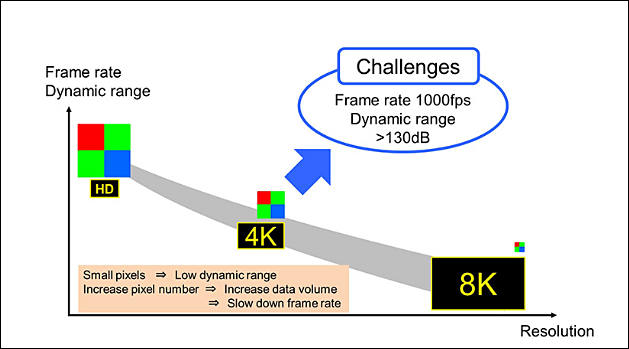
As an optical instrument manufacturer, Nikon is also engaged in research and development of cutting-edge image sensor technology. These efforts build upon Nikon's optical technology, precision measurement / manufacturing technology, and material technology. Currently, image sensors are used not only in imaging field with digital cameras and smartphones, but also in various industrial fields such as automotive. In all fields, there is a demand for image sensors that realize the full combination of compactness, light weight, high frame rate, wide dynamic range, and high resolution.
Image sensor technology development is indispensable for Nikon, and we will continue to research and develop sensors in response to market demands.
Main features
Most advanced level of HDR characteristics of 110 dB and high-speed shooting of 1000 frames per second
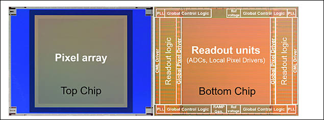
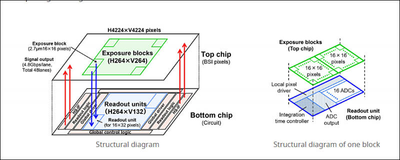
This sensor uses a fine-pitch wafer level wire connection technology consistent with the 2.7 μm pixel size. This makes it possible to control the top chip with the image sensor directly from the logic circuit of the bottom chip. It has a high resolution of 4K × 4K pixels, a wide dynamic range of 110 dB, and high-speed shooting of 1000 frames per second. High-speed readout enables super slow motion shooting of up to 1000 frames per second. It also has a wide dynamic range of 134 dB for shooting 60 frames per second.
Exposure can be controlled for each area on the sensor
The top chip is divided into individual blocks of 16 × 16 pixels, with a total of 264 × 264 blocks (4224 × 4224 pixels) arranged on the sensor. Exposure in each area of the image can be tuned by finely controlling the exposure time of each of the blocks. This is achieved using the bottom chip control architecture.
With this function, users can experience a wide dynamic range, even for subjects with large differences in brightness. Users can clearly shoot the entire scene without crushing the dark areas or overexposing the bright areas.
 sa16632.jpg445 x 297 - 17K
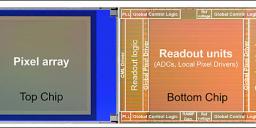 sa16633.jpg635 x 235 - 40K
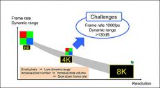 sa16634.jpg629 x 349 - 33K
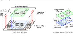 sa16635.jpg800 x 320 - 48K


Howdy, Stranger!
It looks like you're new here. If you want to get involved, click one of these buttons!
Categories
- Topics List23,991
- Blog5,725
- General and News1,354
- Hacks and Patches1,153
- ↳ Top Settings33
- ↳ Beginners256
- ↳ Archives402
- ↳ Hacks News and Development56
- Cameras2,367
- ↳ Panasonic995
- ↳ Canon118
- ↳ Sony156
- ↳ Nikon96
- ↳ Pentax and Samsung70
- ↳ Olympus and Fujifilm101
- ↳ Compacts and Camcorders300
- ↳ Smartphones for video97
- ↳ Pro Video Cameras191
- ↳ BlackMagic and other raw cameras116
- Skill1,960
- ↳ Business and distribution66
- ↳ Preparation, scripts and legal38
- ↳ Art149
- ↳ Import, Convert, Exporting291
- ↳ Editors191
- ↳ Effects and stunts115
- ↳ Color grading197
- ↳ Sound and Music280
- ↳ Lighting96
- ↳ Software and storage tips266
- Gear5,420
- ↳ Filters, Adapters, Matte boxes344
- ↳ Lenses1,582
- ↳ Follow focus and gears93
- ↳ Sound499
- ↳ Lighting gear314
- ↳ Camera movement230
- ↳ Gimbals and copters302
- ↳ Rigs and related stuff273
- ↳ Power solutions83
- ↳ Monitors and viewfinders340
- ↳ Tripods and fluid heads139
- ↳ Storage286
- ↳ Computers and studio gear560
- ↳ VR and 3D248
- Showcase1,859
- Marketplace2,834
- Offtopic1,319


