It allows to keep PV going, with more focus towards AI, but keeping be one of the few truly independent places.
-
No one knows. As all also highly depend on that you do.
Resolve have extremely inefficient architecture, especially GPU part that is aimed at complex unusual workflows, and for typical simple grading it runs at around 1/4-1/5 of possible speed if they did it all proper and using optimized code.
Once I had talk to one developer. It is industry chit chat talks that BM has agreement with some other NLE manufacturers on where they don't go. As if they wanted and aimed at much more beginners and focused on real optimization on FCP X level - they could wipe out all but Adobe.
-
HDMI support
Cards support HDMI 2.1 48GBit/sec and support DSC compression. Maximum supported res is 8K 60Hz with active HDR.
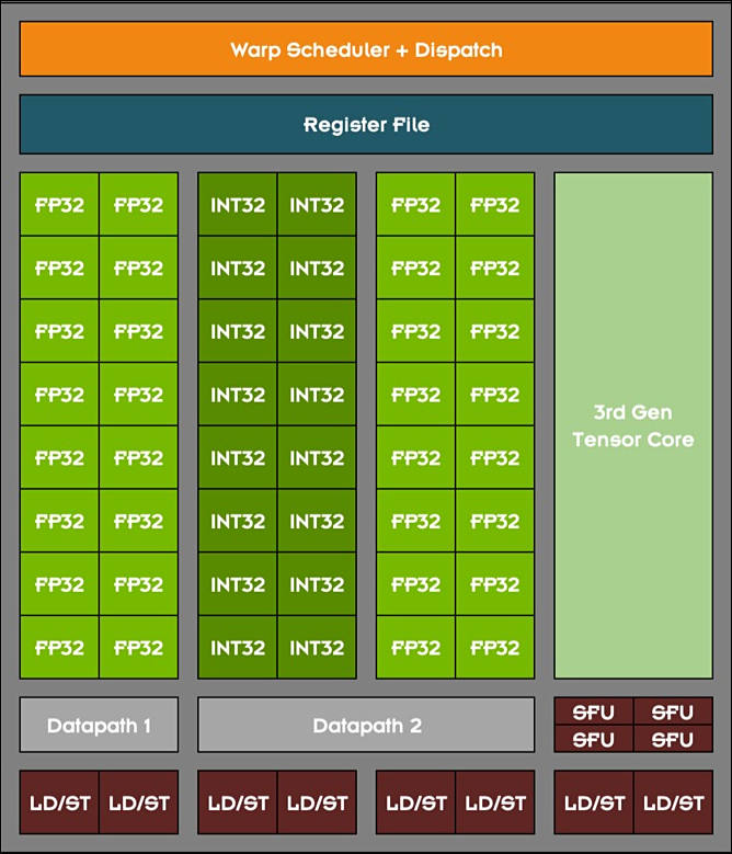
CUDA CORES
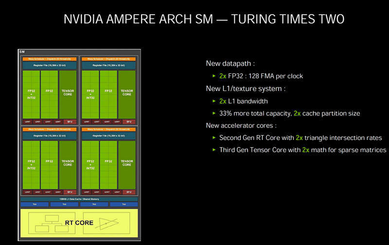
One of the key design goals for the Ampere 30-series SM was to achieve twice the throughput for FP32 operations compared to the Turing SM. To accomplish this goal, the Ampere SM includes new datapath designs for FP32 and INT32 operations. One datapath in each partition consists of 16 FP32 CUDA Cores capable of executing 16 FP32 operations per clock. Another datapath consists of both 16 FP32 CUDA Cores and 16 INT32 Cores. As a result of this new design, each Ampere SM partition is capable of executing either 32 FP32 operations per clock, or 16 FP32 and 16 INT32 operations per clock. All four SM partitions combined can execute 128 FP32 operations per clock, which is double the FP32 rate of the Turing SM, or 64 FP32 and 64 INT32 operations per clock.
Doubling the processing speed for FP32 improves performance for a number of common graphics and compute operations and algorithms. Modern shader workloads typically have a mixture of FP32 arithmetic instructions such as FFMA, floating point additions (FADD), or floating point multiplications (FMUL), combined with simpler instructions such as integer adds for addressing and fetching data, floating point compare, or min/max for processing results, etc. Performance gains will vary at the shader and application level depending on the mix of instructions. Ray tracing denoising shaders are good examples that might benefit greatly from doubling FP32 throughput.
Doubling math throughput required doubling the data paths supporting it, which is why the Ampere SM also doubled the shared memory and L1 cache performance for the SM. (128 bytes/clock per Ampere SM versus 64 bytes/clock in Turing). Total L1 bandwidth for GeForce RTX 3080 is 219 GB/sec versus 116 GB/sec for GeForce RTX 2080 Super.
Like prior NVIDIA GPUs, Ampere is composed of Graphics Processing Clusters (GPCs), Texture Processing Clusters (TPCs), Streaming Multiprocessors (SMs), Raster Operators (ROPS), and memory controllers.
The GPC is the dominant high-level hardware block with all of the key graphics processing units residing inside the GPC. Each GPC includes a dedicated Raster Engine, and now also includes two ROP partitions (each partition containing eight ROP units), which is a new feature for NVIDIA Ampere Architecture GA10x GPUs. More details on the NVIDIA Ampere architecture can be found in NVIDIA’s Ampere Architecture White Paper, which will be published in the coming days.
Lack of progress with encoders
For RTX 30 Series, we decided to focus improvements on the video decode side of things and added* AV1 decode support. On the encode side, RTX 30 Series has the same great encoder as our RTX 20 Series GPU. We have also recently updated our NVIDIA Encoder SDK. In the coming months, livestream applications will be updating to this new version of the SDK, unlocking new performance options for streamers.
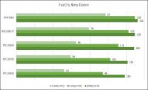
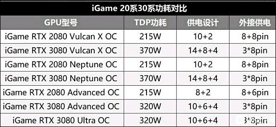
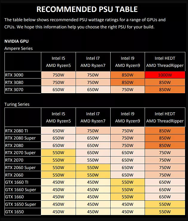
By idea for NLE GPU processing performance must rise 70-80% compared to 2080 Ti (for RTX 2080).
 sa14360.jpg668 x 779 - 95K
 -
As told above it will be in very short supply.
 sa14374.jpg554 x 489 - 39K
 -
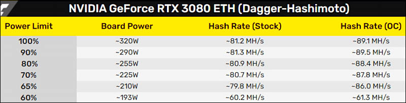
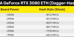
It is one big problem with new RTX cards
Ethereum mining rates are
- RTX 2080 - 40 Mh/s
- RTX 3080 - 115 Mh/s.
In Asia around 90% of all cards go to miners now.
-
 sa14523.jpg727 x 572 - 47K
 sa14524.jpg742 x 540 - 63K
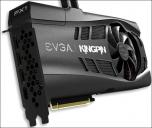 sa14525.jpg667 x 562 - 54K
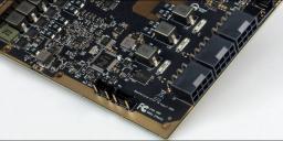 sa14527.jpg800 x 391 - 62K
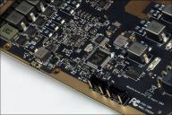 sa14528.jpg800 x 533 - 92K
 -
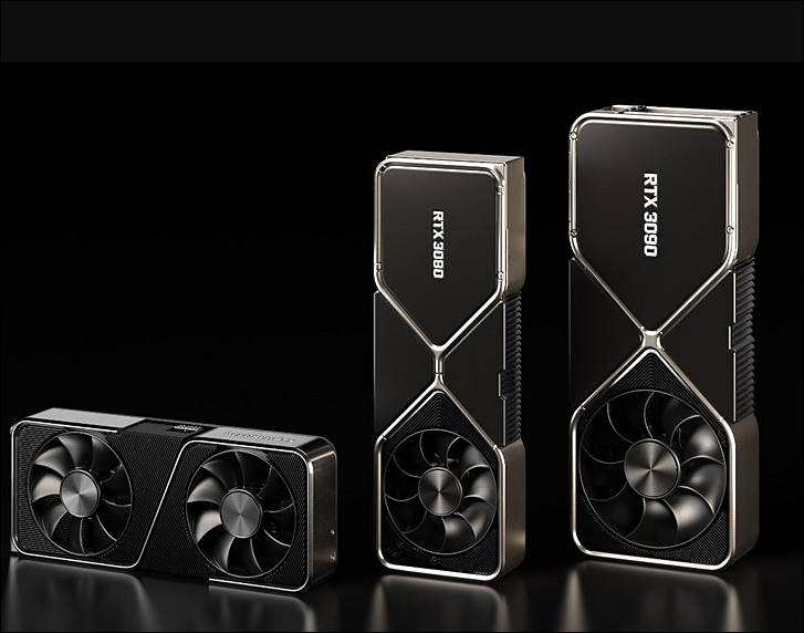
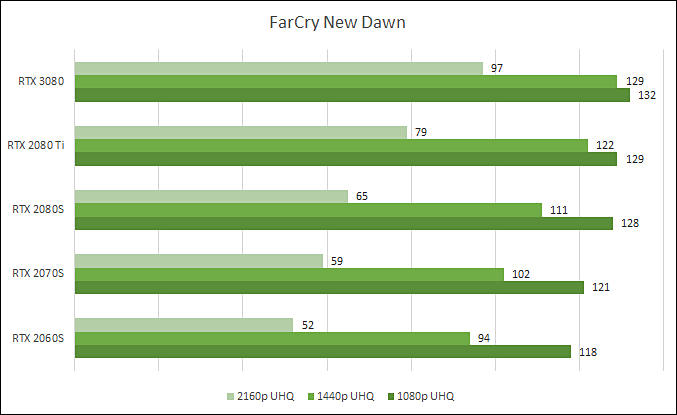
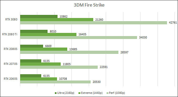
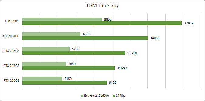
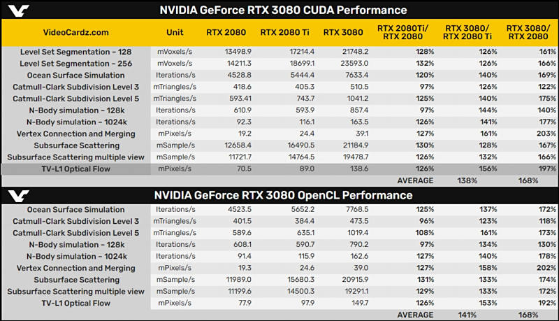
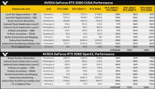
RTX 3080 Benchmarks
- 3DMark Fire Strike Performance: 31919 (+25% к 2080 Ti, +43% к 2080 Super)
- 3DMark Fire Strike Extreme: 20101 (+24% 2080 Ti, +45% 2080 Super)
- 3DMark Fire Strike Ultra: 11049 (+36% 2080 Ti, +64% 2080 Super)
- 3DMark Fire Strike Time Spy: 17428 (+28% 2080 Ti, +49% 2080 Super)
- 3DMark Fire Strike Time Spy Extreme: 8548 (+38% 2080 Ti, +59% 2080 Super)
- 3DMark Fire Strike Port Royal: 11455 (+45% 2080 Ti, +64% 2080 Super)
In average RTX 3080 is 33% faster than RTX 2080 Ti and 54% faster than RTX 2080 Super.
-
3090 ti or a titan based on 3090 should be grate to see its capabilities
-
More leaked benchmarks
 sa14557.jpg677 x 415 - 42K
 sa14558.jpg678 x 371 - 37K
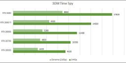 sa14559.jpg675 x 334 - 33K
 -
Good youtube video must be like this one
-
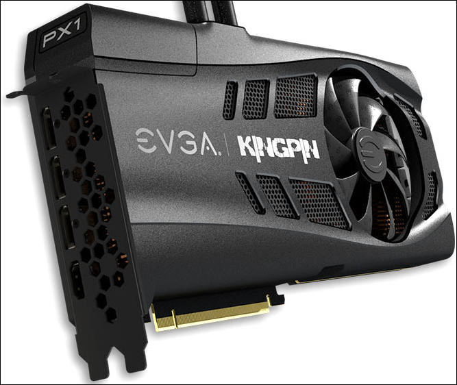
Quadro card based on Ampere will be having less disabled CUDA cores
- GPU GA102 chip
- 10752 fake CUDA cored (actually 5376)
- 1860Mhz clock
- 384 bit memory bus
- 48Gb memory GDDR6
- Quadro A8000 name
Actual number of CUDA cores in GA102 is around 5500, but some can be disabled.
-
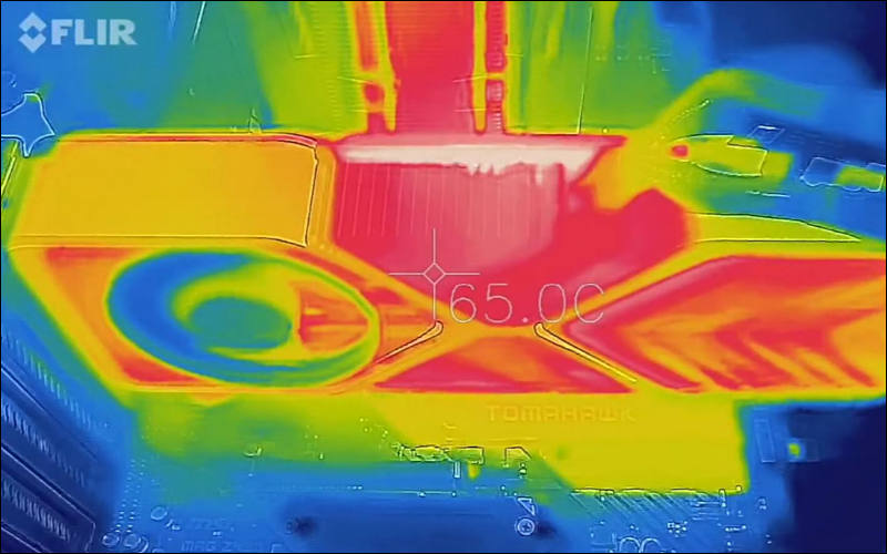
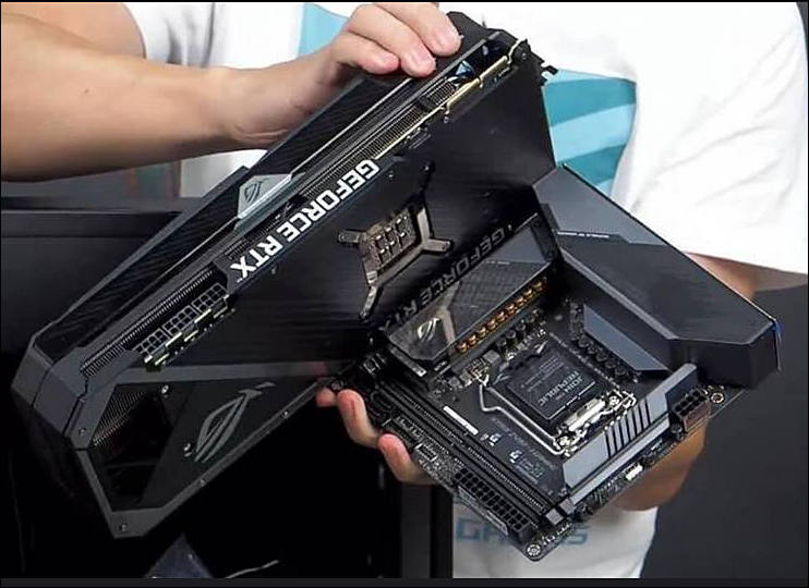
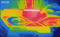
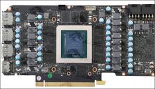
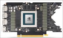
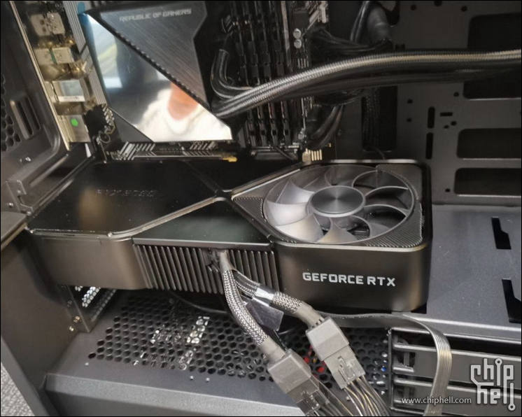
As expected - design of the cooling is not best for 3080 FE.
 sa14589.jpg800 x 500 - 64K
 -
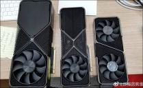
Colorful GPUs
Note how it is first time that better process did not help much.
One guy in industry I talked with told that Ampere GPUs will be very prone to BGA issues and board burnouts. Life of such cards if it is not used with water cooling can be limited to 2 years (if used heavily).
 sa14597.jpg565 x 261 - 43K
 -
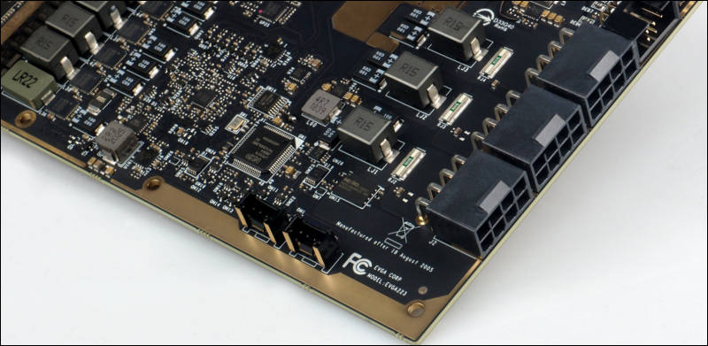
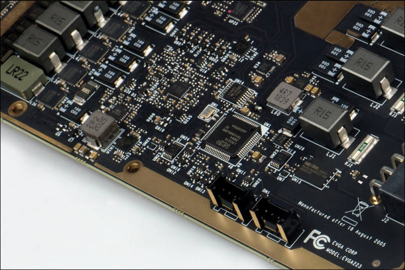
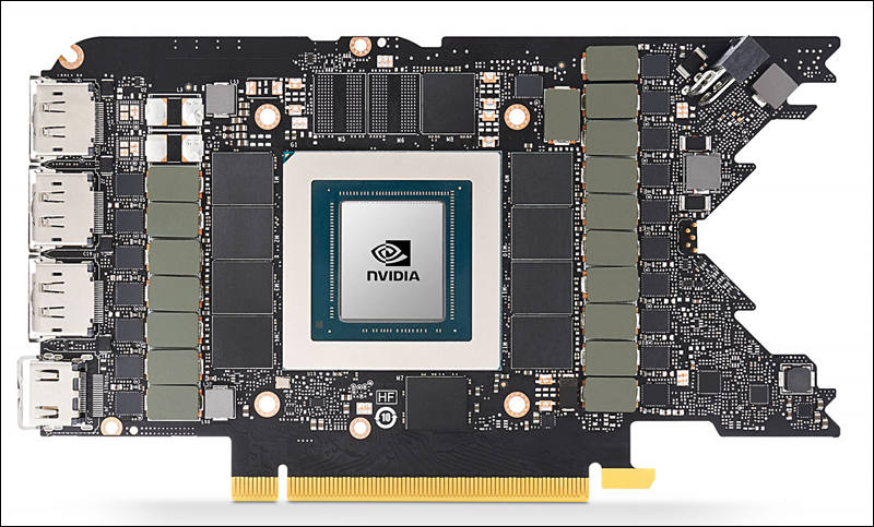
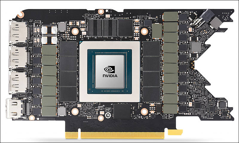
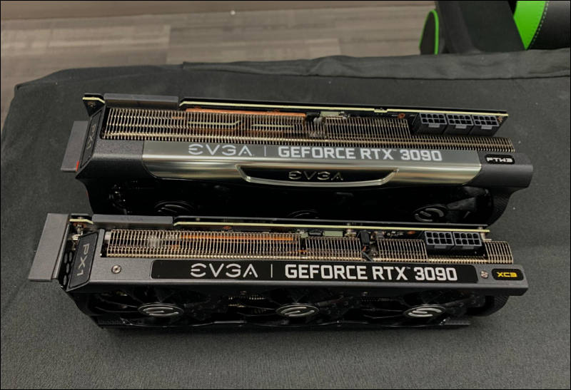
Board design
NVIDIA PG132 reference board for 3080:
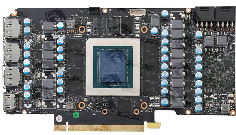
NVIDIA PG132 reference board 3090:
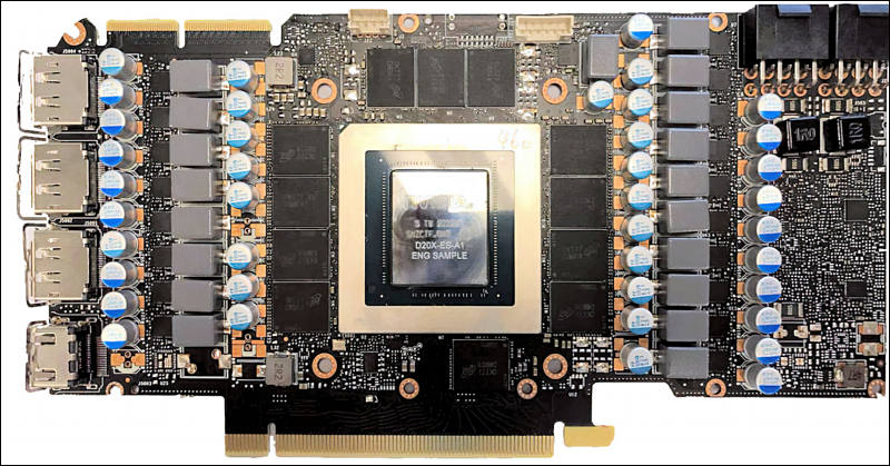
Next time then press will tell you something about very costly top board design and expense on extra memory bus - you can spit them into their prostitute face, as board is literally the same, just less power phases.
NVIDIA PG133 Founders Edition board:
 sa14675.jpg800 x 457 - 91K
 sa14676.jpg800 x 419 - 99K
 sa14677.jpg800 x 483 - 89K


Howdy, Stranger!
It looks like you're new here. If you want to get involved, click one of these buttons!
Categories
- Topics List23,911
- Blog5,718
- General and News1,330
- Hacks and Patches1,148
- ↳ Top Settings33
- ↳ Beginners254
- ↳ Archives402
- ↳ Hacks News and Development56
- Cameras2,342
- ↳ Panasonic984
- ↳ Canon118
- ↳ Sony154
- ↳ Nikon95
- ↳ Pentax and Samsung70
- ↳ Olympus and Fujifilm98
- ↳ Compacts and Camcorders295
- ↳ Smartphones for video96
- ↳ Pro Video Cameras191
- ↳ BlackMagic and other raw cameras116
- Skill1,959
- ↳ Business and distribution66
- ↳ Preparation, scripts and legal38
- ↳ Art149
- ↳ Import, Convert, Exporting291
- ↳ Editors190
- ↳ Effects and stunts115
- ↳ Color grading197
- ↳ Sound and Music280
- ↳ Lighting96
- ↳ Software and storage tips266
- Gear5,407
- ↳ Filters, Adapters, Matte boxes344
- ↳ Lenses1,577
- ↳ Follow focus and gears93
- ↳ Sound496
- ↳ Lighting gear313
- ↳ Camera movement230
- ↳ Gimbals and copters302
- ↳ Rigs and related stuff271
- ↳ Power solutions83
- ↳ Monitors and viewfinders339
- ↳ Tripods and fluid heads139
- ↳ Storage286
- ↳ Computers and studio gear559
- ↳ VR and 3D248
- Showcase1,859
- Marketplace2,834
- Offtopic1,314


