-
To conform to early TV system architectures and other mediums that transmitted data serially, the earliest image sensing technology utilized an electronic shutter mechanism known as a rolling shutter. With this long history, the rolling shutter and its associated columnparallel readout architectures, in which pixels of the same row are readout simultaneously, was also the natural choice for performing shutter operations within CMOS image sensors.
The global shutter pixel technology typically found on charge-coupled device (CCD) image sensors can offer significant benefits such as the elimination of rolling shutter artifacts through simultaneous image capture of the entire frame. However, the use of global shutter pixel requires the addition of a pixel-level memory – one of the barriers to widespread global shutter adoption. As CMOS image sensors have grown in popularity and as machine vision, movie production, industrial, automotive, and scanning applications increasingly place high priority on the ability to capture fast-moving objects with high image quality, image sensor vendors have worked to solve the technical challenges involved with the utilization of global shutter pixel technology on CMOS image sensors -- sensors that were instrumental in making advanced machine vision, scanning, and the filming of movies like Titanic, The Matrix and Avatar1 possible. Further, with significant CMOS processing technology advancements, transistors can be made much smaller; this, together with improved micro-lens technology, is better enabling image sensor vendors to cost-effectively integrate the memory required for a global shutter.
Today, CMOS image sensor providers are closing the performance gap between rolling and global shutter alternatives by addressing several technical challenges -- fill factor/quantum efficiency (QE), global shutter efficiency (GSE), and dark current. In overcoming these challenges, CMOS image sensor vendors are delivering global shutter pixel technology with smaller pixel size, larger fill factor, higher GSE, lower dark current ,and lower noise, better positioning CMOS image sensors to replace CCD at an accelerating rate.
Rolling Shutter Overview
Also known as focal-plane shutter, a rolling shutter utilizes two scans – reset and readout – to control the exposure time. A shutter pulse that resets a row scans the pixel array prior to readout scanning (Figure 1). The interval between the shutter and the readout pulses determines the exposure time. However, since exposure times of different rows are shifted when a rolling shutter sensor is used, still images of fast-moving objects become distorted, rendering the rolling shutter unsuitable for applications like barcode scanning, machine vision, or automated inspection systems, which require the imaging of rapidly moving objects.
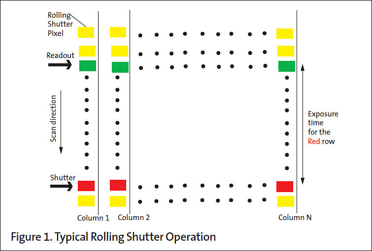
Often found on some film cameras as well as digital still and video cameras using CMOS image sensors, a rolling shutter does not record each frame at a single point in time, but rather captures sequential strips of the image from a vertical or horizontal scan across the frame. The advantage of a rolling shutter method is that the image sensor can continue to gather photons during the acquisition process, thus increasing sensitivity. The disadvantages of rolling shutter - predictable distortion of fast-moving objects or flashes of light, or rolling shutter artifacts - are most noticeable when imaging in extreme conditions of motion or light. The use of rolling shutter technology can also result in other motion artifacts, such as smear, skew, wobble, and partial exposure. A shift from rolling to global shutter has been explored in the past. At the time, CMOS image sensor vendors found that adding an additional memory element would sacrifice too much of the photodiode area, negatively impacting quantum efficiency. Further, with existing semiconductor processing technology, application requirements, market demands, cost, and other considerations, it was not justified to push ahead.
Global Shutter Overview
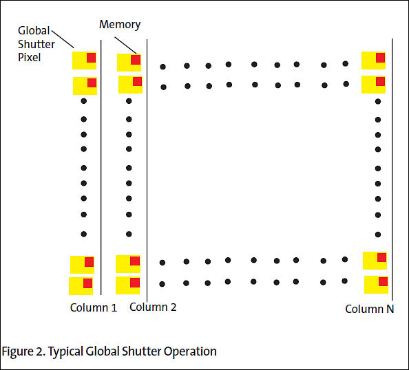
CCD image sensors, which require analog memory for their operation, naturally lend themselves to operation with a global shutter; as a result CCD cameras with global shutter have become more prevalent. The global shutter pixel technology typically found on CCD image sensors used in video cameras eliminates the rolling shutter artifact through simultaneous image capture of the entire frame (Figure 2).
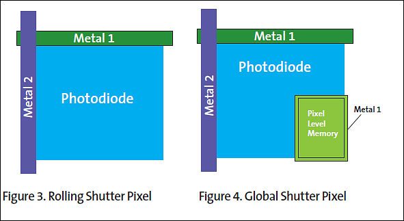
However, for CMOS image sensors, the implementation of a global shutter has the primary disadvantage of requiring the addition of a pixel-level memory, making this an expensive alternative for some applications (Figures 3 and 4). For cost-sensitive mobile applications, in particular, the need for additional pixel-level memory has historically made global shutter undesirable as these applications do not place as high a priority on image quality or the mitigation of rolling shutter artifacts as do other applications, rather for cell phones cost is paramount.
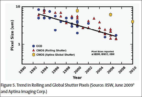
Other drawbacks associated with global shutters include the reduction in pixel fill factor, which results in a decrease in quantum efficiency. To compensate for this effect, a global shutter pixel generally has a larger size than a rolling shutter pixel, as shown in Figure 5.
Another issue of concern is dark current at the memory node. Dark current refers to the small current generated in a pixel even when the pixel is in complete darkness. Typical regions of dark current generation include depletion regions of PN junctions and silicon surfaces. Dark current is one of the main contributors to pixel noise and is more severe in a global shutter pixel than in a rolling shutter pixel.
Finally, it is important to note that, when implementing global shutter in backside illumination (BSI), quantum efficiency is higher than with its front side illumination (FSI) counterpart as there is neither metal nor transistors in the optical path. However, it is this lack of metal that leads to a significant disadvantage for a BSI global shutter. With no metal layer to protect the memory node from light, global shutter efficiency (GSE) is typically degraded. A possible solution is to deposit metal on the backside, but the problem with this is that the resulting stack height is so high that stray light would still be able to contaminate signals stored there. This issue remains an open problem though the industry is exploring it. In the absence of an electronic global shutter, a mechanical shutter can always be used. However, the addition of a mechanical shutter not only increases system cost, but it may be difficult to practically implement in some applications, such as mobile products. Another alternative approach would be to use digital correction of the rolling shutter artifacts; however, this approach would increase power consumption, cost, and may introduce reconstruction artifacts.
CMOS Image Sensors with Global Shutter Technology
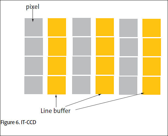
In 2000-2001, it became clear to CMOS image sensor purveyors that global shutter technology could offer significant advantages, but the implementation needed to be carefully considered. The most popular approach that has resulted is “memory-in-pixel,” in which each pixel, in addition to a photodiode and readout circuitry, contains an extra memory element to temporarily store photo-generated charges. In this scheme, every row of the sensor starts an exposure at the same time. At the end of the exposure, photo-generated charges are globally transferred from photo diodes to pixellevel memories and then read out row-by-row via readout scanning. Essentially, the additional pixel-level memory allows photo-generated charge accumulation and readout operation to be performed at each individual pixel, thus eliminating the need for rolling shutter pulses. This approach is similar to that of an Interline-Transfer CCD (IT-CCD) shown in Figure 6, where a line buffer located next to each column of the pixel array serves the same purpose as the in-pixel memory. Since the exposure starts at the same instant for every row, the rolling shutter artifact is not present in this approach. Taking this one step further, by pipelining the accumulation and readout operations, the next exposure can start before finishing the current readout, enabling extremely high frame rates to be achieved.
Fill Factor and Quantum Efficiency
The addition of a memory node in a global shutter pixel causes its fill factor to always be smaller than that of its rolling shutter counterpart. To mitigate reduction in quantum efficiency, such a memory element should occupy as small an area as possible. On the other hand, its charge storage capacity has to be large enough to hold all charge transferred from the photodiode. Ideally, the storage capacity of the memory node should be engineered to be the same as that of the photodiode so that full well of the pixel is not limited by the memory node. Additionally, microlenses should be optimized such that the entire incident light will be collected by the photodiode.
Global Shutter Efficiency
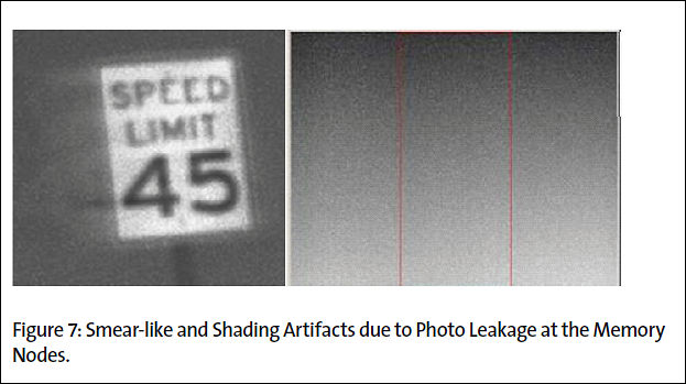
GSE, an important figure-of-merit for a global shutter pixel, is a measure of how well signal charge can be stored in the memory node without being contaminated by parasitic light. GSE measures how well the memory node protects stored signal from parasitic light contamination. Various sources contribute to such a contamination. For example, incident light can never be 100 percent focused onto the photodiode in practice and some may fall onto the memory node due to mechanisms like diffraction and scattering. Figure 7 shows how photo leakage from a bright light hitting the pixel memory during the storage time can affect the stored signal, causing smear-like and shading artifacts.
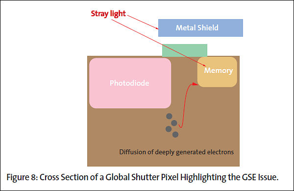
As shown in Figure 8, the memory node acts as a parasitic photodiode that generates electron-hole pairs in response to incident stray light, thus contaminating the signal originally stored there. In addition, electrons generated deep inside the silicon can diffuse into the memory node and act as a second source of signal contamination. To maximize GSE, a metal light shield covering the memory node needs to be used. Additionally, the metal light shield should be as close to the memory node as possible so that the node is protected from stray light arriving at a wide angle. Doping and potential profiles inside the silicon need to be carefully engineered so that stray electrons generated inside the silicon are directed to the photodiode instead of the memory node. Additionally, lenses should be designed such that light is focused as much as possible to the photodiode instead of to the memory node.
Dark Current
With a rolling shutter pixel, charges are accumulated and stored in a low-dark current, surface-pinned photodiode until the pixel is read out. In contrast, a global shutter pixel has to store accumulated charges in a memory node commonly implemented in silicon. For example, in a 2003 study by Krymski and Tu2, the floating diffusion of a pixel was used as a memory node. Similar to a 3-T photodiode, there is a large leakage current associated with the surface even though the pixel is in complete darkness. Additionally, the fact that the floating diffusion needs to be a heavily doped junction results in a large PN junction leakage current which acts as another source of dark current. This highly undesirable dark current contaminates the signal stored in the memory node. To mitigate this, a process should be developed to passivate or pin the surface of the memory node. Instead of using a floating diffusion as a memory element, Aptina has utilized a surface-pinned storage node in the pixel to address dark current challenges. Available in its newest global shutter sensor, the MT9M031, the storage node also enables using a true correlated double sampling technique to reduce readout noise to four electrons, resulting in excellent low-light performance. The combination of the effective use of an anti-reflective metal light shield in close proximity to the memory node and careful doping and potentialprofile design results in a high GSE. Charge storage capacities of the photodiode and the memory node are also balanced, and when taken together with the use of a two-way shared pixel architecture, the impact of the memory node on fill factor and QE is minimized. The combination of all these engineering innovations is a 3.75 micron global shutter pixel that enables high performance without rolling-shutter artifacts.
Via: http://www.aptina.com/products/technology/Aptina_Global-Shutter-WhitePaper.pdf
-
Despite: "However, it is this lack of metal that leads to a significant disadvantage for a BSI global shutter. With no metal layer to protect the memory node from light, global shutter efficiency (GSE) is typically degraded. " I think BSI is the answer.
http://www.faqs.org/patents/app/20090201400
Global shutter requires more electronics in front of the photo diode which lowers quantum efficiency of the sensor. One alternative is BSI (back side illuminated) sensor, where electronics are placed behind the photo diode. http://www.aptina.com/news/FSI-BSI-WhitePaper.pdf
BSI sensor efficiency could be up to 90% compared to pro DSLRs with their 60% QE using FSI. http://en.wikipedia.org/wiki/Back-illuminated_sensor
BSI gotchas are: the pixel density needs to be really high @ 1.1 micron to be that efficient and they are very expensive atm. We will see smaller sensors taking advantage of it first. It's already in your iPhone 4s and bunch of P&S cameras. Currently all major players have patents for BSI related tech.
Sony has it's "Exmor R": http://www.sony.net/SonyInfo/technology/technology/theme/exmor_r_01.html
-
This is an awesome post. I eat this stuff up and as I do, a million new ideas come to mind. I believe 99.9% of them are completely illogical because of material science, but they seem like awesome ideas right now. Carry on!
-
Great post, but I have a question about Figure 7. Assuming the image of the speed limit sign was taken from a moving car, the sign would have been travelling from left to right in the field of view. The ghosting in the image is taking place to the left of the speed limit sign, so logically it would be a trailing edge effect rather than a leading edge effect. Parasitic light sensitivity, or GSE as you called it in your post, is typically a leading edge effect. Image lag is a trailing edge effect caused when less than 100% of the electrons don't move from the photodiode to the memory. Do you agree, or am I missing something?
-
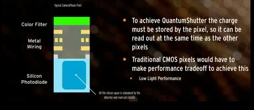
I wonder if this "Quantum Shutter" sensor has got anywhere yet since July 2011 when it received the International Imaging Industry Association’s (I3A) VISION 2020 Imaging Innovation’s top gold award.
Rolling Shutter:

Standard CMOS - Global Shutter
Quantum Shutter
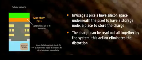
from http://www.invisageinc.com/page.aspx?cont=QuantumShutter
 Skew.png480 x 270 - 144K
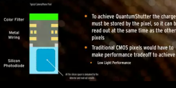 cmos.png503 x 219 - 110K
 Screenshot.png496 x 211 - 97K


Howdy, Stranger!
It looks like you're new here. If you want to get involved, click one of these buttons!
Categories
- Topics List23,991
- Blog5,725
- General and News1,354
- Hacks and Patches1,153
- ↳ Top Settings33
- ↳ Beginners256
- ↳ Archives402
- ↳ Hacks News and Development56
- Cameras2,367
- ↳ Panasonic995
- ↳ Canon118
- ↳ Sony156
- ↳ Nikon96
- ↳ Pentax and Samsung70
- ↳ Olympus and Fujifilm101
- ↳ Compacts and Camcorders300
- ↳ Smartphones for video97
- ↳ Pro Video Cameras191
- ↳ BlackMagic and other raw cameras116
- Skill1,960
- ↳ Business and distribution66
- ↳ Preparation, scripts and legal38
- ↳ Art149
- ↳ Import, Convert, Exporting291
- ↳ Editors191
- ↳ Effects and stunts115
- ↳ Color grading197
- ↳ Sound and Music280
- ↳ Lighting96
- ↳ Software and storage tips266
- Gear5,420
- ↳ Filters, Adapters, Matte boxes344
- ↳ Lenses1,582
- ↳ Follow focus and gears93
- ↳ Sound499
- ↳ Lighting gear314
- ↳ Camera movement230
- ↳ Gimbals and copters302
- ↳ Rigs and related stuff273
- ↳ Power solutions83
- ↳ Monitors and viewfinders340
- ↳ Tripods and fluid heads139
- ↳ Storage286
- ↳ Computers and studio gear560
- ↳ VR and 3D248
- Showcase1,859
- Marketplace2,834
- Offtopic1,319


